flying591
Newbie level 3
problem about LDO!
hi everyone
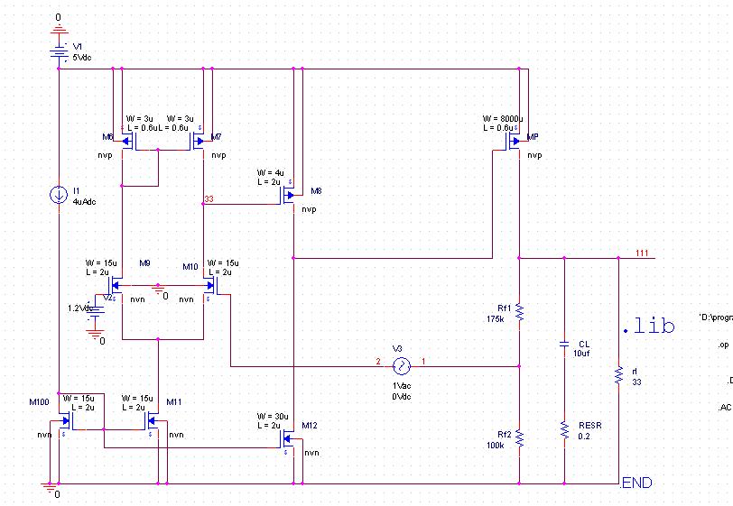
In a LDO circuit, I change the value of the ESR resistance, it should only change the zero which is generated by Resr.but at some values it not only change the zero bu also change the pole. moreover,the changed pole has imaginary part.
why??
for this pole,how compensation?
thanks in advance for any response that may help me!
hi everyone
In a LDO circuit, I change the value of the ESR resistance, it should only change the zero which is generated by Resr.but at some values it not only change the zero bu also change the pole. moreover,the changed pole has imaginary part.
why??
for this pole,how compensation?
thanks in advance for any response that may help me!