Continue to Site

Welcome to EDAboard.com

Welcome to our site! EDAboard.com is an international Electronics Discussion Forum focused on EDA software, circuits, schematics, books, theory, papers, asic, pld, 8051, DSP, Network, RF, Analog Design, PCB, Service Manuals... and a whole lot more! To participate you need to register. Registration is free. Click here to register now.

Power PCB Track width ideas

Status
Not open for further replies.

SBTECH

Newbie level 6
Joined
Feb 17, 2010
Messages
12
Helped
0
Reputation
0
Reaction score
0
Trophy points
1,281
Location
Istanbul, Turkey
Activity points
1,390
Dear All,

I am designing a relay switching board whick will switch 230 V AC 5A Motors. In my PCB Design, I am trying to use one layer 2 oz/ft^2 copper.


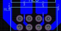
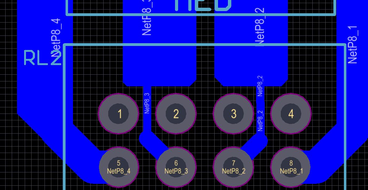
I am just guessing if such a routing as in the attachement is dangerous or not ? For 5A current , I need to have 100 mil tracks. But between relay's contact i had to do such a routing. For example for NetP8_3, I started with 50 mil width from Pad 6 and routed for 3.5 mm length , then routed for 3.5 mm length with 25 mil track width , than i continue with a polygon pour.

Do you think that cause any problems ?

Thanks very much for all your helps..
 

That narrowing will create a drop voltage, maybe inexpressive.
However, you must consider the electro-magnectic induction effect, due to too much close distances.

Some things must be measured empirically to account destructive effect, but I sugest don´t do that.


+++
 

I would download the Saturn PCB toolkit and look at fusing currents..
Im with Andre on this one, I would be concerned.

Best option would be to change the pin out of the connector if possible, or trim down the unused pads to bet thicker traces betweeen them and use two traces per connection.
 
Last edited:

Motor wiring should also consider inrush currents. Apart from this problem, the geometry should be O.K. for 5 A. In terms of expectable trace heating, a short thinner segment isn't that critical. The design is most likely not O.K. related to required clearance. IPC2221 is e.g. requiring 0.4 mm under permanent coating or 1.25 mm uncoated for 230 VAC. According to other safety standards (e.g. IEC1010) even higher clearance is reuqired according to overvoltage categories of mains voltage.

Practically, there's no reasonable option to route traces between the relay pads. I don't know what's the electrical connection of the upper pad row, perhaps they can be connected to the power circuit?


SBTECH,


If pins RL2:2 / RL2:3 are unused, what about you connect tracks to those nets, instead avoid them ?
This way, you could increase minumum distances, and even route with a regular width.


+++
 

pin2 and pin3 are belong to other contacts of the relay , and relay is switching 230V ac , so when there is no power on the relay coil , there is 230V on that pins(2 and 3) , when i power the coil pin 6 and others powered with 230V . I found another solution by designing this pcb with two layers.

Where can i learn about this IPC2221 and IEC safety standards especially for power boards , as you know when designing normal microcontroller boards without RF , designer is more free when placing the components and tracing , But I should learn about PCB design standards, or could you please recommend me some books about professional PCB design?

I am really a fresh engineer and universities are not giving lectures about pcb design in our country :) ,

Thanks very much for your helps EDABOARD community !
 

Once those pins 2,3 are not used, could be created a new relay footprint, not using them.
Remember to insert a step in board assembly instruction to perform the 2,3 pins cutting.

This way, the region under that pins would be avaliable to route.


+++
 
Last edited:

Or perhaps even better, change the relay for another one that does allow you to route out of it with adequate widths tracks and clearance from the pins.
 

Status
Not open for further replies.

Part and Inventory Search

Welcome to EDABoard.com

Sponsor

Back
Top