mickey0908
Junior Member level 2
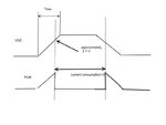
would anyone please tell how design a power on reset circuit in the condition of vdd from 2.3 to 5.5 ,and the delayed time is 20us . thanks !!!
Follow along with the video below to see how to install our site as a web app on your home screen.
Note: This feature may not be available in some browsers.
IanP said:**broken link removed**
Regards,
IanP
butterfish said:IanP said:**broken link removed**
Regards,
IanP
this poweron have two problem:
1> it can not work if vdd rise too slowly, for this, need large R&C;
2> on the other hand, if R,C are too large, glitchs on vdd will trig RESET, means
circurt will be reset time to time;
butterfish said:IanP said:**broken link removed**
Regards,
IanP
this poweron have two problem:
1> it can not work if vdd rise too slowly, for this, need large R&C;
2> on the other hand, if R,C are too large, glitchs on vdd will trig RESET, means
circurt will be reset time to time;
surianova said:butterfish said:IanP said:**broken link removed**
Regards,
IanP
this poweron have two problem:
1> it can not work if vdd rise too slowly, for this, need large R&C;
2> on the other hand, if R,C are too large, glitchs on vdd will trig RESET, means
circurt will be reset time to time;
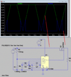
the glitch problem can be solved if you use internal voltage regulator to power up the POR. Your regulator must have good PSRR.
iamxo said:butterfish said:IanP said:**broken link removed**
Regards,
IanP
this poweron have two problem:
1> it can not work if vdd rise too slowly, for this, need large R&C;
2> on the other hand, if R,C are too large, glitchs on vdd will trig RESET, means
circurt will be reset time to time;
you said so good!
but how did you know this?
I work in submicron cmos process with a supply voltage equal to 2.5 V.
I use Cadence IC.
The main problem is that there should be zero current consumption (no more 10nA) when the supply voltage established