Continue to Site

Welcome to EDAboard.com

Welcome to our site! EDAboard.com is an international Electronics Discussion Forum focused on EDA software, circuits, schematics, books, theory, papers, asic, pld, 8051, DSP, Network, RF, Analog Design, PCB, Service Manuals... and a whole lot more! To participate you need to register. Registration is free. Click here to register now.

Power Factor Correction (PFC with boost): Average current mode Control

Fianso97

Newbie
Joined
Nov 22, 2023
Messages
3
Helped
0
Reputation
0
Reaction score
0
Trophy points
1
Activity points
34
Hello everyone,

I'm currently writing my Bachelor thesis on the subject mentioned in the title and I'm having some problems understanding the control part although i have read a lot of papers and application notes.

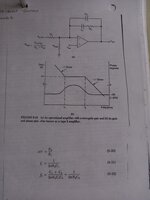
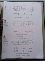
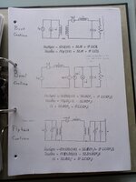
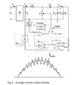
I generally understand how the circuit works (from a power electronics point of view) and I know that there are 2 loops: a current loop (type 2) and a voltage loop (type 1) so that the input current follows the rectified voltage in order to . I find it hard to understand how to calculate the values of R and C in these loops according to the transfer function of the boost + the 2 transfer functions of the loop. My Professor has provided me with the boost transfer function and the small signal equation (attached)but I still don't know how to use this transfer function...

Can anyone who has done this or something similar give me a step by step guide? i would appreciate it very much.
 

Attachments

  • Compensation zero-pole pair.jpg
    Compensation zero-pole pair.jpg
    846.1 KB · Views: 50
  • Transfer Functions - Current Mode.jpg
    Transfer Functions - Current Mode.jpg
    856.9 KB · Views: 46
  • Transfer Functions - Continuous Mode.jpg
    Transfer Functions - Continuous Mode.jpg
    867.1 KB · Views: 52
This simulator taught me about power factor error and how to implement pf correction. Ampere levels are elevated because the inductive load introduces a phase change which is typical of inductors. Articles state that this doesn't require the AC generator to work harder but it does require all wires be thicker, making everything more expensive.

Choose the capacitor value so that it resonates at the supply frequency with the inductive load. Simultaneously the benefit is to reduce Ampere levels through the system.

power factor error simulations ( before and after correction).png
 
Thanks for your reply! the problem that i posted handels the active power correction not the passive as you have mentioned. i have an ac input + bridge rectifier + boost+ feedback loop thta controls the duty cycle of the mosfet.. here is a picture that demonstrate how it works
Screenshot 2023-11-22 173939.png

This simulator taught me about power factor error and how to implement pf correction. Ampere levels are elevated because the inductive load introduces a phase change which is typical of inductors. Articles state that this doesn't require the AC generator to work harder but it does require all wires be thicker, making everything more expensive.

Choose the capacitor value so that it resonates at the supply frequency with the inductive load. Simultaneously the benefit is to reduce Ampere levels through the system.

View attachment 186356
 
Hi,

The OP is not clear in this, but I guess the OP talks about an AC/DC power supply module with PFC stage.

@OP:
Please provide a sketch of the circuit you are talking about.
Then tell us what you understand so far and where you need our assistance.

In none of your circuits I see AC at all.
But power factor correction is related to AC. Usually grid power sine waveform. (Again guessed)

Klaus
hank you for your response. I am indeed referring to an AC/DC power supply module, consisting of a single-phase bridge rectifier, boost PFC, and load.

I acknowledge the presence of two loops:

  1. Current Loop (Main Loop): This involves a sense resistor (Rs) to measure the voltage across it. The resulting voltage is then compared with the product of the voltage error and the input voltage (rectified). The outcome drives the MOSFET gate to maintain the input current in phase with the input voltage.
I have already designed the components of the boost circuit (L, C, fs, Vin, Vout). Now, I'm seeking guidance on designing the control loops. Despite reviewing various papers and application notes, I find the equations in the Laplace domain confusing.

I understand the necessity of small-signal modeling to obtain the required transfer functions. However, the multitude of equations seems chaotic. I wish to gain a clearer picture of the overall process
 

Attachments

  • Screenshot 2023-11-24 122555.png
    Screenshot 2023-11-24 122555.png
    41.1 KB · Views: 45

LaTeX Commands Quick-Menu:

Part and Inventory Search

Welcome to EDABoard.com

Sponsor

Back
Top