Continue to Site

Welcome to EDAboard.com

Welcome to our site! EDAboard.com is an international Electronics Discussion Forum focused on EDA software, circuits, schematics, books, theory, papers, asic, pld, 8051, DSP, Network, RF, Analog Design, PCB, Service Manuals... and a whole lot more! To participate you need to register. Registration is free. Click here to register now.

PLZ help with this switching circuit

Status
Not open for further replies.

EDA_hg81

Advanced Member level 2
Joined
Nov 25, 2005
Messages
507
Helped
2
Reputation
4
Reaction score
2
Trophy points
1,298
Activity points
4,808
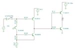
I try using this circuit to switch 0.2V and 0V to output.
The first NPN and PNP for realizing the control level shift to compensate the Vbe of second PNP.
How do you think this circuit?
I have run TINA and it can work but not sure if it still can work in real world.
Many thanks in advance.
 

Attachments

  • TRY.JPG
    TRY.JPG
    29.7 KB · Views: 107

Apart from looking unnecessarily complex and using arbitrary high base currents, the circuit should work. Strictly spoken, the 74HCT specification won't guarantee reliable operation of the first stage with 200 ohm resistors.

The minimum requirement is to have a negative gate voltage. A minimal circuit may be comprised of the 74HCT driver, two resistors, a negative supply and the two output transistors, I think.
 
Sincere thanks for your answers.
I originally plan to use 74ACT04 since it has higher output current but there is no model for 74ACT04 in TINA so I have to use 74HCT04 model instead.
If it is possible would you show your simplified level shift circuit?
One more question:
When T3 is connected GND to output VF1, should any current flow through VCE of T3, I am really confusing about this.

Many thanks.
 
Last edited:

Status
Not open for further replies.

Similar threads

Part and Inventory Search

Welcome to EDABoard.com

Sponsor

Back
Top