chomix05
Newbie level 5
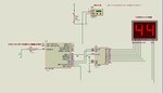
DIGITAL THERMOMETER
schematic diagram

Code:
list p=16f628
#include <p16f628.inc>
errorlevel 0,-302
CBLOCK 0x20
DS_DAT
DS_SIGN
DUMMY0
DUMMY1
DUMMY2
DUMMY3
DUMMY4
SEND
COUNT
NUM1
NUM2
NUM3
DATA1
HALF
endc
#define DAT_PIN PORTB,0 ; 74595 DATA pin
#define LATCH PORTB,4 ; 74595 LATCH pin
#define CLK PORTB,5 ; 74595 CLK pin
#Define DQ PORTA,0
org 0x000
goto Start
Table_ addwf PCL,f
dt 0x3f,0x06,0x5b,0x4f,0x66,0x6d,0x7d,0x07,0x7f,0x6f
Start clrf PORTA ; Set port A for digital I/O
movlw 0x07
movwf CMCON
bsf STATUS,RP0
movlw b'00000110' ; Set port B for displaying via LED 7 segments
movwf PORTB
bcf STATUS,RP0
Main call RD_Temp ; Read data from DS1820
clrf HALF ; A Half digit
bcf STATUS,C
rrf DS_DAT,w ; Use 7-bit upper
rlf HALF,f ; Store a half degree
movwf DATA1 ; Data for convert to decimal
call Convert ; Convert data to decimal
call Delay3 ; Display data delay
goto Main
;**********************************************************************
; Display On 7 Segment *
;**********************************************************************
Delay3 clrf DUMMY4 ; Display data delay
DelayLp call Disp
decfsz DUMMY4,f
goto DelayLp
return
Delay2 clrf DUMMY3 ; Delay for scanning LED 7 segments
decfsz DUMMY3,f
goto $-1
return
Disp movf NUM1,w ; Load data to DSP1
call Table_ ; Convert
btfsc HALF,0 ; Show a half degree on dot-point LED
addlw 0x80
call Send_Dat ; Send data to LED 7 segments
bcf PORTB,6 ; ON DSP1 Display
call Delay2
bsf PORTB,6
movf NUM2,w ; Load data to DSP2
call Table_ ; Convert
call Send_Dat ; Send data to LED 7 segments
bcf PORTB,7 ; On DSP2
call Delay2
bsf PORTB,7 ; Off DSP2
return
Send_Dat movwf SEND ; Load data
movlw 0x08 ; Loop 8 times for sending 8-bit data
movwf COUNT
Chk_Bit bcf DAT_PIN ;
btfsc SEND,7 ; Check bit 7 "0" or "1"
bsf DAT_PIN ; Send bit 7 to shift register
Clock bsf CLK ; Clock pulse
bcf CLK
Rotate rlf SEND,f ; Rotate bit for sending next bit
decfsz COUNT,f ; Test loop 8 times ?
goto Chk_Bit ; If no, send bit again
Latch bsf LATCH ; Latch data for displaying
bcf LATCH
return
;**********************************************************************
; Macro for DS1820 *
;**********************************************************************
DQLOW macro
bcf DQ ; DQ bit ready
bsf STATUS,RP0
bcf DQ ; Set DQ to output
bcf STATUS,RP0
endm
DQHIZ macro
bsf STATUS,RP0
bsf DQ ; Set DQ to input
bcf STATUS,RP0
endm
PAUSE macro DELAY ; Generate delay time
movlw DELAY
movwf DUMMY0
call Delay5
endm
;**********************************************************************
; DS1820 1-Wire bus *
;**********************************************************************
RD_Temp call DS_Rx ; Check chip status
addlw 0x01
btfss STATUS,Z ; Z set = ready
return ; W is not zero = not ready
Get_Temp call DS_Reset
movlw 0xcc ; Skip ROM
call DS_Tx
movlw 0xbe ; Read scratch pad RAM of DS1820
call DS_Tx
call DS_Rx ; Read 8-bit data
movwf DS_DAT
call DS_Reset ; Restart
movlw 0xcc ; Skip ROM
call DS_Tx
movlw 0x44 ; Start conversion
call DS_Tx
Delay5 nop ; Delay for PAUSE macro
nop
decfsz DUMMY0,f
goto Delay5
return
DS_Reset DQLOW
PAUSE 0x77 ; 600 microcsecond delay
DQHIZ
PAUSE 0x0c ; Wait for response pulse (67 microsecond)
nop
nop
movf PORTA,w ; Read response
andlw 0x01 ; Use RA0 only
movwf DUMMY1
PAUSE 0x3b ; 300 microcsecond delay
movf DUMMY1,w ; Response in W
return
DS_Tx movwf DUMMY2 ; Transmission data
movlw 0x08 ; Prepare 8-bit counter for sending data
movwf DUMMY1 ; Define loop counter
Tx_Loop DQLOW ; Macro of DQ pin to low, This is start bit
PAUSE 0x01 ; 10 microsecond delay
rrf DUMMY2,f ; Rotate data to Carry flag
btfsc STATUS,C ; Test Carry flag
bsf DQ ; If Carry flag = "1" , set DQ to high
PAUSE 0x0d ; 70 microsecond delay
DQHIZ
nop
decfsz DUMMY1,f ; 8 times ?
goto Tx_Loop ; No, send again
return
DS_Rx movlw 0x08 ; Recieve 8-bit data
movwf DUMMY1
Rx_Loop DQLOW ; Macro of DQ pin to low, this is start bit
PAUSE 0x01 ; 10 microsecond delay
DQHIZ ; Back to high for receiving
nop
nop
movf PORTA,w ; Read data
andlw 0x01 ; Get data bit 0 only
addlw 0xff ; Move data bit 0 to Carry flag with addition method
rrf DUMMY2,f ; Move data bit 0 to DUMMY bit 7
PAUSE 0x0b ; 60 microsecond delay
decfsz DUMMY1,f ; Loop 8 times
goto Rx_Loop ; Read again
movf DUMMY2,w ; Save data to W register
return
;**********************************************************************
; Convert Hex to Decimal (3 Digit) *
;**********************************************************************
Convert clrf NUM2 ; Clear register of 10's unit
Check movlw 0x0A ;
subwf DATA1,w ; Subtract with 10 until lower 10
btfss STATUS,C ; Check subtraction result lower 10 ?
goto Less1 ; If yes then return
incf NUM2,f ; If no, increase 10's unit value
movlw 0x0A ;
subwf DATA1,f ; Subtract with 10 until lower 10 and check result again
goto Check
Less1 movf DATA1,w ;
movwf NUM1 ; Send data to 1's unit display
clrf NUM3 ; Check hundred unit
Check2 movlw 0x0A
subwf NUM2,w ;
btfss STATUS,C ; 10's unit over 10 ?
return ; If no then return
incf NUM3,f
movlw 0x0A ; If yes, subtract again and check until the result is lower 10
subwf NUM2,f
goto Check2
;**********************************************************************
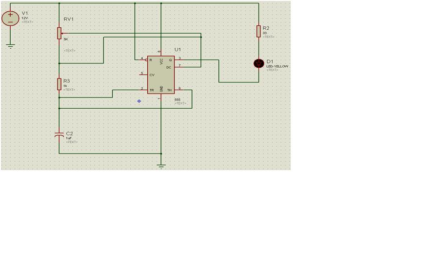
endschematic diagram
When you post code use CODE tags [alexan_e]
Last edited by a moderator: