Continue to Site

Welcome to EDAboard.com

Welcome to our site! EDAboard.com is an international Electronics Discussion Forum focused on EDA software, circuits, schematics, books, theory, papers, asic, pld, 8051, DSP, Network, RF, Analog Design, PCB, Service Manuals... and a whole lot more! To participate you need to register. Registration is free. Click here to register now.

[SOLVED] Please Check My N-Channel MOSFETs H-Bridge Schematic Diagram

Status
Not open for further replies.

thir13enth

Member level 1
Joined
Feb 23, 2011
Messages
38
Helped
4
Reputation
8
Reaction score
4
Trophy points
1,288
Location
Quezon City, Philippines
Activity points
1,545
Purpose: PWM Controlled Vehicle
Rating: 20A+ & 12V-24V
-------------------------------

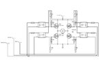
I have attached here a schematic diagram taken from my design in Proteus. It works good on Proteus and hopefully, it would be working when we implement it on hardware.

Please check it if I am missing something which I should include upon doing the hardware. We are planning to buy the materials ASAP, your suggestions are very welcome!

:-D
 

Attachments

  • PWM H-Bridge.jpg
    PWM H-Bridge.jpg
    51 KB · Views: 256
Last edited:

I think you should read something like **broken link removed**

First of all a mosfet needs a proper driver that can provide current to be able to switch fast or the mosfet losses will be high (heat) especially with PWM which will be in KHZ rate, using the 1K gate 10K gate to source are very high anyway.

The second problem is that in order to use Nmosfet in the high part of the bridge (instead of Pmosfet that doesn't have that problem) you need a higher power supply voltage source for the gate or a bootstrap circuit to generate that higher voltage.
The problem is that you need a gate voltage that is higher than the source pin but as the mosfet turns on the source pin will have almost the same voltage as the drain (12v) so your Vgs bias will be almost 0 (12v gate, 12v source).

Read the pdf, it has everything you need.

Alex
 
Last edited:
Thank you Sir alexan_e for your reply.

I have used an optocoupler. This component functions like switching a LED inside and then activating the transistor inside. Meaning, if I have 12V, I will also have 12V as input for my gate. Will that be okay?
 

No it is not OK,
The problem is that you need a gate voltage that is higher than the source pin and when the mosfet turns on the source pin will have almost the same voltage as the drain (12v) so your Vgs bias will be almost 0 (12v gate, 12v source).

Read page 20 "High side direct drivers for N-channel devices" from the PDF link of my previous post.

Alex
 

The gate voltage seems okay on the hardware. The only problem is that, when one of the upper side gates is switched, the other one also turns on.

What would be the reason?
 

I can only assume that you haven't read the reference I gave you

"a high side switch necessitates a gate drive circuit
which is referenced to the source of the
MOSFET. The driver must tolerate the violent
voltage swings occurring during the switching
transitions and drive the gate of the MOSFET
above the positive supply rail of the power
supply
. In most cases, the gate drive voltage must
be above the highest DC potential available in the
circuit
.

Alex
 

I did and I also tried it, yet the motor did not run when I did that... so I sticked to the original design which is functioning yet, the two side of the bridge is switching simultaneously.

---------- Post added at 02:46 ---------- Previous post was at 02:42 ----------

I also tried isolating the upper from the lower bridge, and the problem still exists.
 

Let me show you exactly what the problem is in a simplified circuit with a high side Nmosfet

nmosfet_high_side.gif

You mosfet has an RDSon of 0.005 ohm and should have almost 0 voltage drop across drain-source but you can clearly see that you have a voltage drop of 3v because this is the balance point for this mosfet that has an low gate threshold (1V).
Also take a look at the numbers in the same circuit with IRF640 which has a gate threshold of about 3v, notice the 6v voltage drop across drain-source

Now calculate the power consumption over that mosfet using 3v multiplied with the 20A+ output current, you are looking at 60W of heat (or 120W for IRF640), do you see the problem.

nmosfet_high_side_correct.gif

Now check the numbers in my second schematic where an isolated voltage source is applied to the gate, see how the losses are minimal, 0.05v for IRL2203 and 1v for IRF640 (because it has higher ON resistance).
You can either do it with an isolated power supply, an available power supply with higher voltage from the one that the mosfet uses or using bootstrap technique.

Note that the losses in both cases are static, when you add switching loses it will get worse.

Now your control problem, I assume that you wanted to connect all cathodes to the enable line and then two diagonal anodes (Q1/Q4) to one direction and the other two (Q2/Q3) to the reverse direction, it should solve your problem.

Alex
 

Thank you for your time.

I tried to isolate the the motor source (12V) and the gate source (14V) and did the second picture on your post, yet the upper bridge is still switching simultaneously.

Also I tried 5V as motor source and 12V as gate source, yet the motor did not move.

If there is still something I have to consider, please do tell me.
 

What alex is trying to say is your high side mosfet need to be saturated, that's why you need a boost trap circute,which is right when using N-channel mosfet.
 

Sorry but I really cannot fully understand. There is no problem activating the IRL2203. The problem lies when activating one of the high side, the other also activates. ><

The lower side works well, only the high side gives a problem of simultaneous activating.
 

You can still use your mosfet what i am saying is your diagram will not work the way you want.
 

Thank you for your time.

I tried to isolate the motor source (12V) and the gate source (14V) and did the second picture on your post, yet the upper bridge is still switching simultaneously.

The isolated power supply was to show you how to drive the mosfets properly, the solution for your control problem was in this part

Now your control problem, I assume that you wanted to connect all cathodes to the enable line and then two diagonal anodes (Q1/Q4) to one direction and the other two (Q2/Q3) to the reverse direction, it should solve your problem.

I though that by showing you the voltage drop on the mosfet using your driving method and the amount of heat would change your mind but for some reason you still don't see the problem.
You circuit can't be done with just a few components, you need at least 2 additional driver for your mosfets (one for each HI/LO mosfet) or if you use discrete driver components many more.
I guess you'll have to make the real circuit to understand what we are talking about.

Alex
 

I guess you'll have to make the real circuit to understand what we are talking about.

Alex

Well, I thought I was receiving pieces of information to help me with my circuit. But it turned out to be NOT. BTW, I am making the real circuit on the breadboard and I am doing the things you have told me.

I tried posting my original schematic design on the other forum. One guy told me that my R5 and R8 are pull up resistors, which should not be. It will cause to saturate my upper bridge MOSFETs simultaneously which is exactly what my problem is. Thus, I made these pull up resistors as pull down resistors since I am using N-Channel MOSFETs.

Alas! It worked. The motor is forwarding and reversing as well as the PWM. The MOSFETs are showing very minimal heat when I turned the circuit for 15 minutes. I have tried many complicated tests and yet the problem is only at the pull up resistors. Funny, it is.

I am now marking the thread as solved. Thanks for the help!
 

Status
Not open for further replies.

Part and Inventory Search

Welcome to EDABoard.com

Sponsor

Back
Top