Continue to Site

Welcome to EDAboard.com

Welcome to our site! EDAboard.com is an international Electronics Discussion Forum focused on EDA software, circuits, schematics, books, theory, papers, asic, pld, 8051, DSP, Network, RF, Analog Design, PCB, Service Manuals... and a whole lot more! To participate you need to register. Registration is free. Click here to register now.

plane/pours help in Altium

Status
Not open for further replies.

manishyamdagni

Junior Member level 2
Joined
Oct 15, 2004
Messages
20
Helped
0
Reputation
0
Reaction score
0
Trophy points
1,281
Activity points
109
Hi All,
can anyone tell me how to generate a copper pour/ plane so that they connect through thermal ties only on smt pads and full connected(no thermals) with via and through holes
Thanks in advance
Regards
 

Hi,
Follow the below Steps,
First to place polygon go to Place/polygon pours, select the required amount of area to pour polygon.
Then go to design their select polygon connect style rule and different rules for pad and via.
For Pad --- pass query IsPad
For Via-----Pass query IsVia
For SMT pad to pass query as IsSmtPin
 
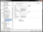
Open your design rules. Under Polygon Connect Style add something like the following:
SMT.JPGThruPin.JPGVia.JPG
 

Status
Not open for further replies.

Part and Inventory Search

Welcome to EDABoard.com

Sponsor

Back
Top