Continue to Site

Welcome to EDAboard.com

Welcome to our site! EDAboard.com is an international Electronics Discussion Forum focused on EDA software, circuits, schematics, books, theory, papers, asic, pld, 8051, DSP, Network, RF, Analog Design, PCB, Service Manuals... and a whole lot more! To participate you need to register. Registration is free. Click here to register now.

PIN diode having similar attributes to SRD in 130nm GF for frequency multipliers

Status
Not open for further replies.

Samraz

Newbie level 2
Joined
Aug 2, 2018
Messages
2
Helped
0
Reputation
0
Reaction score
0
Trophy points
1
Activity points
16
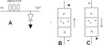
In my simulations PIN diode when chosen so small(1um x 1um) behave similarly to SRD. I saw similar post in EDA. Is it possible that 'I' region is kind of similar to 'n' region of srd when the device is small. Is there anyway to very the model of devices. Besides in GF process model guide, the PIN diode model is so comprehensive . Thanks
 

Unfortunately the model doesn't cover completely charge control effect and at best they can be used as frequency doublers. I simulated using TCAD and then got totally different results.
 

Yeh, dont trust spice models. I was excited when I simulated an Infineon BAR63 pin diode. I got like 10V/ns, but when I made the circuit, a schottly diode was faster...
 

PIN diodes and SRD diodes are the same thing, although an SRD might have a slightly different doping profile to enhance harmonic generation.

In B, you see a PIN or SRD, where + voltage is applied to the P terminal. Electrons dance their way across the I region, since it is a forward biased diode.

In C, you see the same diode, where - voltage is applied to the P terminal. For a short while, the electrons that are in the I region reverse direction and the diode current appears to be reversed. in other words, even though the diode is reverse biased, it is conducting current...momentarily. After the LAST of those electrons gets swept out of the I region, the terminal current abruptly goes to ZERO. But that current was being supplied thru and inductor. So as the current goes to zero, the inductor generates a spike of VOLTAGE to try to keep the current flowing.

That spike of voltage has a lot of harmonic energy in it....and hence acts like a frequency multiplier if the input terminal has a large sine wave drive
 

Attachments

  • srd.JPG
    srd.JPG
    10 KB · Views: 96

Status
Not open for further replies.

Part and Inventory Search

Welcome to EDABoard.com

Sponsor

Back
Top