savethewales
Newbie level 1
Hi Everyone,
i'm trying to make piezoelectric pump which includes a piezoelectric disk and a driving board.
unfortunately my knowledge of electronics is only slightly more than zero so i need some professional advice.
in general i want to replicate the driving board which looks like this:
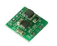
from description:
...It converts a single 2.5 - 6 VDC power and generates a drive voltage of 215 Vp-p at frequency of around 40 Hz...
...power consumption 100mW...
regular sine wave is acceptable.
So I see 5 components. Can anybody suggest the wiring scheme between this 5 components with values assigned to them?
If U1 is microcontroller what kind of signals should it generate (sine wave is required in the end)?
Any ideas are very welcome
Thanks