abc123
Member level 4
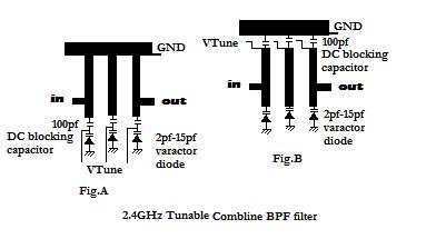
I have a question on the PCB layout of a 2.4GHz tunable combline BPF filter,
It is tunable by changing the voltage of varactor diodes. see the attached picture. There are two possible implementations, Fig.A and Fig.B since the tuning voltage Vtun can not shorted to GND, I need a DC blocking capacitor between the varactor diode and Microstrip lines which is grounded.
the questions is which way is better ? Fig.A or Fig.B
The PCB layout of Fig.A is a little bit messy, Is the series capacitor and diode, may change the length of Microstrip line ?
For the fig.B arrangement what is the DC blocking capacitor should be for varactor diode in 2.4GHz? is the 100pf capacitor good enough to ground the Microstrip line in 2.4GHz frequency?
 [/img]
It is tunable by changing the voltage of varactor diodes. see the attached picture. There are two possible implementations, Fig.A and Fig.B since the tuning voltage Vtun can not shorted to GND, I need a DC blocking capacitor between the varactor diode and Microstrip lines which is grounded.
the questions is which way is better ? Fig.A or Fig.B
The PCB layout of Fig.A is a little bit messy, Is the series capacitor and diode, may change the length of Microstrip line ?
For the fig.B arrangement what is the DC blocking capacitor should be for varactor diode in 2.4GHz? is the 100pf capacitor good enough to ground the Microstrip line in 2.4GHz frequency?