sgaltium
Member level 2
Hi,
Need Altium expertise help or give some advises on below problem.
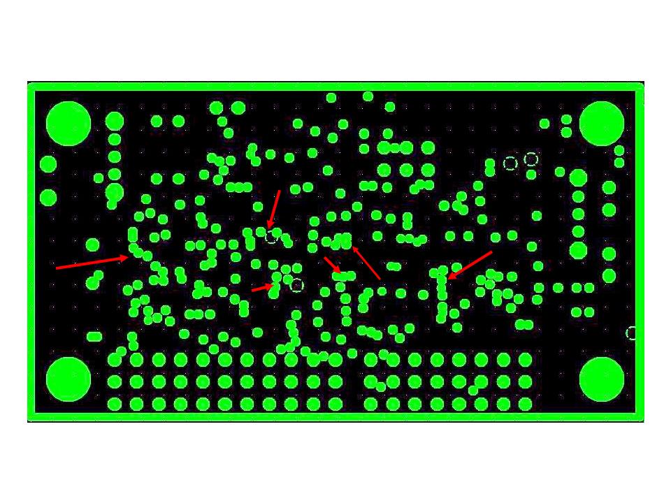
Board Design:
4 layers board design
Top and bottom layers with components
Second layer = +5v
Third layer = GND
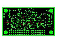
Please refer attached screenshot.
or
https://obrazki.elektroda.pl/89_1304038742.jpg
I'm using auto routing method.
In every layer, some of the pad and via stack together, any solution for this problem? Any setting can prevent this happen during auto routing?
Appreciate your kindly reply. Thanks.
Need Altium expertise help or give some advises on below problem.
Board Design:
4 layers board design
Top and bottom layers with components
Second layer = +5v
Third layer = GND
Please refer attached screenshot.
or
https://obrazki.elektroda.pl/89_1304038742.jpg
I'm using auto routing method.
In every layer, some of the pad and via stack together, any solution for this problem? Any setting can prevent this happen during auto routing?
Appreciate your kindly reply. Thanks.