analog_ambi
Member level 1

Hi,
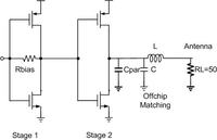
I am designing a PA as shown in schematic. Some specs are:
2.4 GHz
ultra low power (<1mA)
moderate linearity (modulation is QPSK, moderate PAR, either class A or class AB)
The problem is my gain falls by 2dB (w.r.t mid band gain) at 2.4GHz when O/P is loaded with 200f parasitic capacitance. The O/P shall drive offchip matching network and then 50 ohm. I have the following questions:
1. How do I get fair estimate of parasitic cap Cpar (bond pad+bond wire+ package pad+ pcb)
2. Is it possible to tune the parasitic cap out by including it in the cap (C) of matching network.
3. If yes then onchip or offchip cap for matching solves it best? The matching network upconverts 50 ohm to 500 ohm.


