vijith133
Member level 1

Hi,
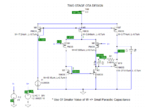
I am designing a simple two stage OTA as show in the figure. can anyone suggest the test bench for simulating the transconductance of the OTA.
Pls do explain with figures if possible. I tried looking into lot of test benches already uploaded but it did not make much of sense to me.
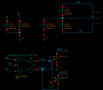
ex: https://www.edaboard.com/threads/248195/
but mine is a single ended output OTA these figure in the link mentioned was confusing for me, and also the Cmref output. I could not understand what it was.
I am designing a simple two stage OTA as show in the figure. can anyone suggest the test bench for simulating the transconductance of the OTA.
Pls do explain with figures if possible. I tried looking into lot of test benches already uploaded but it did not make much of sense to me.
ex: https://www.edaboard.com/threads/248195/
but mine is a single ended output OTA these figure in the link mentioned was confusing for me, and also the Cmref output. I could not understand what it was.