Continue to Site

Welcome to EDAboard.com

Welcome to our site! EDAboard.com is an international Electronics Discussion Forum focused on EDA software, circuits, schematics, books, theory, papers, asic, pld, 8051, DSP, Network, RF, Analog Design, PCB, Service Manuals... and a whole lot more! To participate you need to register. Registration is free. Click here to register now.

OpAmp - Negative Feedback operation

Status
Not open for further replies.

shaikss

Full Member level 4
Joined
Jun 18, 2007
Messages
229
Helped
1
Reputation
2
Reaction score
1
Trophy points
1,298
Activity points
3,319
Hi Folks,

I was going through some analytical paper on Opamps and got a doubt regarding the -ve feedback operation.
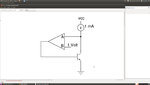
I have attached the circuit.
The Q is to label which of the terminals 'A' and 'B' are +ve and -ve so that the entire circuit works in -ve feedback.

Let me explain how I analysed the circuit,
Here terminal B is fixed to 1V and the current source of 1mA is driving the collector of BJT.
For me, it looks like a current monitor circuit.
So, I feel that the terminal which is connected to collector should be inverting terminal and so terminal A should be inverting terminal to make the circuit work in negative feedback mode.

Am I correct?
If wrong, Please correct me and let me know how to analyse the circuit.

Thanks!
 

Attachments

  • Screenshot-2.png
    Screenshot-2.png
    78.1 KB · Views: 66

So, I feel that the terminal which is connected to collector should be inverting terminal and so terminal A should be inverting terminal to make the circuit work in negative feedback mode.

Hi shaikss,

no, the terminal A has to be non-inverting to establish negative feedback.
Explanation: A rising opamp output voltage causes further opening of the transistor. This leads to a falling collector potential and compensates the output increase.

---------- Post added at 13:49 ---------- Previous post was at 13:27 ----------

I suppose it could be useful (if not necessary) to increase the reference voltage to ensure proper BJT operation.
 

...label which of the terminals 'A' and 'B' are +ve and -ve so that the entire circuit works in -ve feedback.
Am I correct?
Hi Shaikss,
Terminal "\'A' should be non inverting to make the loop in -ve f/b. Transitor always have negative polarity from BJT's , Base to collector.(check y). So 'A' should be +ve terminal.
Next, in this circuit, opamp infact used to dc bias the BJT and provide CM.
 

So, I feel that the terminal which is connected to collector should be inverting terminal and so terminal A should be inverting terminal to make the circuit work in negative feedback mode.

Hi shaikss,

no, the terminal A has to be non-inverting to establish negative feedback.
Explanation: A rising opamp output voltage causes further opening of the transistor. This leads to a falling collector potential and compensates the output increase.

---------- Post added at 13:49 ---------- Previous post was at 13:27 ----------

I suppose it could be useful (if not necessary) to increase the reference voltage to ensure proper BJT operation.

Hi LvW,

Can you please explain me in detail?

---------- Post added at 05:21 ---------- Previous post was at 05:19 ----------

---------- Post added at 05:21 ---------- Previous post was at 05:21 ----------

Hi Shaikss,
Terminal "\'A' should be non inverting to make the loop in -ve f/b. Transitor always have negative polarity from BJT's , Base to collector.(check y). So 'A' should be +ve terminal.
Next, in this circuit, opamp infact used to dc bias the BJT and provide CM.

Hi Varunkant2k,

I didn't understand. Can you explain me how to analyse it?
 

assume terminal A is at 5V. clearly higher than terminal B's 1V. if A is the inverting input, then the opamp's output should go as low as possible -- preventing the transistor from turning on at all. This is a stable state. Likewise, if A were 0V, and B were 1V, then the opamp would force as much current into the base as it could, turning the transistor on fully -- again a stable state. indeed, this would be a latch.

Now assume in the 5v/1v example that A were non-inverting. the transistor would turn on, forcing the terminal away from 5V. Likewise in the 0v/1v case, the transistor would turn off allowing the voltage to rise. This would be the correct action.

Thanks permute. Now, I understood.
Can you suggest me some text book where i can solve this kind of problems?
 

the 3rd edition sedra-smith book (microelectronic circuits) is good in general, though might be a bit rigorous if you are looking for something lighter. It does have a lot of questions on opamps as well as feedback. Basic opamp circuits have plentiful literature on TI/national/maxim-ic/analog's websites. Basically any company that makes opamps.

this circuit is often called the "simulated zener", or the "shunt regulator".
 

You can find some suggestions for Op Amp literature in

Recommendations for Op Amp Books

The second paragraph contains a link to "Op Amps for Everyone" from Texas Instruments which is quite good (and freely avaialable).

I would also second permutes suggestion of Sedra / Smith, they have lots of exercises. But I think the latest edition is the 6th, not the 3rd.


---------- Post added at 05:21 ---------- Previous post was at 05:19 ----------

---------- Post added at 05:21 ---------- Previous post was at 05:21 ----------


Hi Varunkant2k,

I didn't understand. Can you explain me how to analyse it?

Hi Please read transistor operation. If you get voltage response from base to collector in Common Emitor configuration..you will get it.
 

Status
Not open for further replies.

Similar threads

Part and Inventory Search

Welcome to EDABoard.com

Sponsor

Back
Top