Continue to Site

Welcome to EDAboard.com

Welcome to our site! EDAboard.com is an international Electronics Discussion Forum focused on EDA software, circuits, schematics, books, theory, papers, asic, pld, 8051, DSP, Network, RF, Analog Design, PCB, Service Manuals... and a whole lot more! To participate you need to register. Registration is free. Click here to register now.

OpAmp feedback issue

Status
Not open for further replies.

Foyevtsov

Newbie level 4
Joined
Jan 5, 2015
Messages
6
Helped
0
Reputation
0
Reaction score
0
Trophy points
1
Activity points
56
Hi, analog guys :)

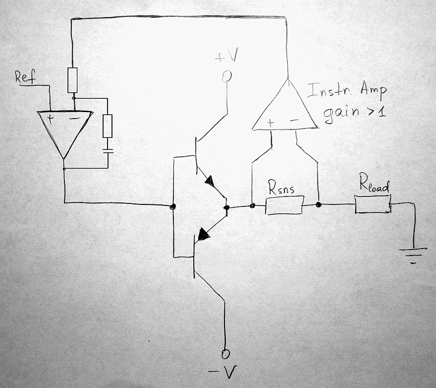
I am working on some schematics and came to the point where I am getting troubles, which I don't know how to to explain/deal with. I believed that the following scheme (see the picture) should work. Should it? If no, then why, if yes, then what should be a stupid mistake it doesn't? (I mean the most stupid mistakes, like wrong connections, I've already checked).

P.S. If some other details are needed, just tell.

IMG_0818.JPG
 

Dear SunnySkyguy, maybe I am a super stupid guy :), but are is there any reason this sketch should not work?
 
Last edited:

What do you expect from the circuit? What means "should work"?
 

Ok, fare enough.

It is assumed to drive predefined current to the R_load, while the value of the current is set by a corresponding voltage on the Ref pin. The purpose of the instrumentation amplifier (to the right) with the sensing resistor R_sns is to convert current to voltage and to provide the negative feedback to the OpAmp (to the left).

The higher the voltage output on the OpAmp the higher the current through R_sns, then the higher the voltage output on the Instr.Amp and, hence, the higher the input voltage on the negative input of the OpAmp. Thus, providing a proper feedback. Shouldn't this be the case or I'm missing something?
 

The circuit is usually called a bipolar current source. But you missed to tell about the problems you experience. The circuit has correct feedback polarity and should basically work.

For a practical design, there are several point to consider like amplifier common mode range and stability requirements. It should be also noted that the class B output stage causes crossover distortions.
 

By connecting the negative input of the OpAmp directly between the R_sns and R_load (basically making a voltage source) the scheme works fine. In this configuration, the current sense part gives correct readings and everything works as expected.

But once I move to the current source (the scheme on the plot) the OpAmp loads the Ref (Ref is a low-resistance source, or, simply another OpAmp) and starts drawing some 5 mA in it. The inputs of the OpAmp are then at different potentials, but the output is far from being saturated. So, I am wondering if the sketch shows a generally correct scheme, because I checked the connections many times and those look okay.
 

The rails are -12V and +12V for OpAms, Instr.Amp, and the transistors. The OpAmp on the scheme is NE5534, the Instr.Amp is INA826. Transistors are Darlington ones so the OpAmp drives them easily in the required range (base currents up to 1 mA). The Ref voltage is DC and lays within +- 2.5V.

I actually changed today NE5534 with a simple LM224 and the current feedback works with the last one. But I am wondering now what is so different between these two?

"Loop phase margin" - have to look in that. Does it have something to do with the frequency compensation of NE5534? I thought it should be relevant only for AC signals, but could this be that a transient process together with some characteristics of NE5534 prevent the circuit from settling?

Thanks for the hint
 

Some more details necessary:
- amplifier types
- amplifier power supply

A possible problem is that the circuit could be oscillating due to insufficient loop phase margin.

- - - Updated - - -

NE5534 has input clamping diodes which will conduct e.g. if the circuit is oscillating.

It's clearly a problem of loop frequency compensation. You are cascading to amplifiers in the feedback loop which is only possible with well considered compensation. NE5534 with external compensation option is a special case, usually you would trim the loop gain by adding a RC circuit that reduces the loop gain at higher frequencies with an I or PI characteristic.
 
FvM, thanks for the advice! I searched a bit into the topic of frequency compensation, which is honestly a new to me, and made some good! I adjusted my scheme with the idea presented in https://cms.edn.com/ContentEETimes/Images/EDN/Old%20figures/One%20extra%20resistor%20fights%20IC%20op-amp%20oscillations/One_extra_resistor_fights_IC_op_amp_oscillations_figure_2.jpg
... and now it works. Some of the OpAmps in the whole scheme were indeed oscillating, thus, corrupting the results. Now, I can get linear voltage-to-current characteristics for simple resistors using the whole scheme (so it works :) ).

Thanks to those who helped! ... and shame to those who didn't... joking :)
 

Status
Not open for further replies.

Similar threads

Part and Inventory Search

Welcome to EDABoard.com

Sponsor

Back
Top