Continue to Site

Welcome to EDAboard.com

Welcome to our site! EDAboard.com is an international Electronics Discussion Forum focused on EDA software, circuits, schematics, books, theory, papers, asic, pld, 8051, DSP, Network, RF, Analog Design, PCB, Service Manuals... and a whole lot more! To participate you need to register. Registration is free. Click here to register now.

op amp stability question

Status
Not open for further replies.

KonstanU

Member level 5
Joined
Jun 7, 2012
Messages
82
Helped
28
Reputation
56
Reaction score
27
Trophy points
1,298
Location
Bayreuth, Germany
Activity points
1,719
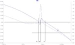
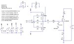
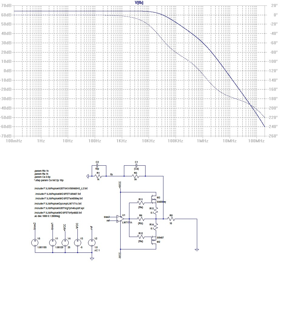
I know when amplifier is unstable. But I have got the next picture of amplifier loop gain (FB is open).
Loop gain.jpg

So is this picture stable or not?
 

As far as I can see (the picture is very hard to read) - the phase reaches 0 deg for a loop gain magnitude>0.
Thus, after closing the loop the circuit will be unstable.
 

Thank you.
Lets I make picture more readable.
I have non-inverting amplifier and I apply AC signal on the non-inverting input of op amp.

On the picture I have indicated three frequencies at which loop gain passes through G=1.
f1 = 6.5 Mhz (PM = 100)
f2 = 9 Mhz (PM = 160)
f3 = 18 Mhz (PM = 50)

It looks like stable but I have doubts.
 

Attachments

  • Loop gain2.jpg
    Loop gain2.jpg
    56.4 KB · Views: 72
Last edited:

Application of amplifier is a bite strange.
It is used as the Gate Driver with adjusted voltage.
I have connection of OpAmp and current boost stage.

In practice I have oscillation and I think that the reason for that could be multi-poles system.
 

Attachments

  • Circuit.Loop gain.jpg
    Circuit.Loop gain.jpg
    94.5 KB · Views: 70

In practice I have oscillation and I think that the reason for that could be multi-poles system.
In practice, small signal analysis doesn't describe the system behaviour completely. The most severe point is the class B current boost stage where both MOSFETs are off for the calculated bias point. In addition MOSFET and IGBT capacitances are strongly voltage dependent. The OP might add non-linear behaviour.

As far as linearity can be assumed, bode diagram stability analysis should still work for the present circuit. I wonder however where the "dip" around 10 MHz can be localized in the circuit.
 

Hi FVM,

Wont it be the self resonating frequency of the inductors use
 

I have checked simulation model.
I can state that induction is not the reason of unstability.
I have simplifed my load and what I have got you can see on the following pictures.


Results reveal that external current boost creates additional poles and zeros that make system unstable.
 

The question is if the non-feedback current booster in the second circuit is meeting your design specifications?

In addition to my previous post, I see that you biased the class B buffer by a DC input voltage and a load resistor in your simulation circuit. This point can't be guessed from your previous posts. If the setup gives a realistic representation of the real load situation is a different question.

I also notice that Ra and Rb have considerable high values, thus MOSFET capacitances matter a lot.
 
Status
Not open for further replies.

Similar threads

Part and Inventory Search

Welcome to EDABoard.com

Sponsor

Back
Top