Continue to Site

Welcome to EDAboard.com

Welcome to our site! EDAboard.com is an international Electronics Discussion Forum focused on EDA software, circuits, schematics, books, theory, papers, asic, pld, 8051, DSP, Network, RF, Analog Design, PCB, Service Manuals... and a whole lot more! To participate you need to register. Registration is free. Click here to register now.

Op amp circuit explanation

Status
Not open for further replies.

zuser999

Newbie level 6
Newbie level 6
Joined
Jul 8, 2013
Messages
12
Helped
0
Reputation
0
Reaction score
0
Trophy points
1
Location
LA
Visit site
Activity points
99
Hello all,

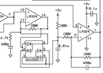
I have these op amp that I don't seem to understand. I've went through several articles about op amps and didn't find any that were similar to what I have in the circuit attached. Can someone please explain me what is the each stage? and how it done.

Thank you
 

Attachments

  • Screen Shot 2013-07-08 at 3.40.31 AM.png
    Screen Shot 2013-07-08 at 3.40.31 AM.png
    65.6 KB · Views: 126

op amp are used to produce the output of voltages for the input voltage but with an operation executed... such as in inverting Vout=-Vin(Rf/Rin) and in non inverting Vout=Vin(1+Rf/Rin).... and we can make both to do the sum, difference, product etc.... your circuit is small part of the whole... with my knowledge i understand only small part.... and BAY99DW is the protection unit or isolation unit... the circuit is noise filter and followed by amplifier by stage by stage... it is clear that the resistor and capacitor connected forms the filter unit and LM324 as amplifier.... it will more visible if whole circuit is posted....
 

I just want to know in detail what exactly the second stage and the third stage are doing. I doubt the BAY99DW is just for protection or isolation; it is doing something else. As for the third stage, I'm having difficulty in analysing the circuit. A bit of help is appreciated.
 

The second-stage LM324 appears to be a peak detector. The diode 2 is to compensate for the voltage drop of diode 5, which charges the 0.01uF capacitor to the negative peak voltage from the first stage.

Diode 1 is a clamp for positive voltages to prevent the op amp from saturating.

Diode 4 does nothing as it is shorted out.

The third-stage LM324 is apparently an inverting buffer amp for the peak signal.
 

This is ustrasonic range finder. Transducer is transmitter and receiver for echo sound. First two OPAs are AC amplifiers and antiparallel diodes at the second OPA negative feedback serve for signal amplitude limiting both positive and negative. Third diode from the output of second OPA is envelope detector whose signal is inverted in third OPA and feed to PIC.
Delay between transmited signal and received signal is measure for distance to object of interest.
 
Can it be that the stage 2 op amp is acting as a log amplifier and not a peak detector?
 

Can it be that the stage 2 op amp is acting as a log amplifier and not a peak detector?
Not particularly. The diode limiter is performing a kind of logarithmic dynamic compression. But the circuit's purpose is to detect the echo's rising edge, ideally independent of it's magnitude.

I basically agree with explanations by crutschow and Borber.
 
To summarize of what I understood is that the antiparallel diodes are clamping the signals, both the positive and the negative cycles, and the diode 5 is acting as a peak detector for the negative edges. Is that true?

One thing I noticed is that the 2.7kOhm and the 680pF form a highpass filter that has a corner frequency of 86KHz, but the receiving signal is @40KHz. How is this possible? The 40KHz signal will be attenuated dramatically.

Thanks
 

The 40KHz signal will be attenuated dramatically.
It reduces the maximum (unclamped) gain only. And not "dramatically" because the maximum gain is already limited by LM324 bandwidth.
 

The full gain will be only achieved as long as the output voltage is below +/- diode threshold.
 

Status
Not open for further replies.

Similar threads

Part and Inventory Search

Welcome to EDABoard.com

Sponsor

Back
Top