Continue to Site

Welcome to EDAboard.com

Welcome to our site! EDAboard.com is an international Electronics Discussion Forum focused on EDA software, circuits, schematics, books, theory, papers, asic, pld, 8051, DSP, Network, RF, Analog Design, PCB, Service Manuals... and a whole lot more! To participate you need to register. Registration is free. Click here to register now.

one side of IR2110 full bridge mosfets burns instantly

Status
Not open for further replies.

farid72j

Junior Member level 3
Joined
Jul 29, 2021
Messages
26
Helped
0
Reputation
0
Reaction score
0
Trophy points
1
Activity points
208
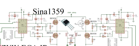
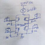
I have build a full bridge inverter using 2 IR2110 and 4 irf840 or 20n60 mosfets. pwm frequency of high side is 18 kHz and for the low side i use 50 Hz pulse. the circuit works fine with 25 and 50 volt from dc supply.
the problem is when i connect 310 v dc of rectifying 220 v ac to the circuit, 2 mosfet on one side burns instantly.

i use different mosfets and dead time up to 2 ms, the result is the same.
can someone tell me where is the problem?
thank you in advance.
 

Attachments

  • SinaInverterPureSineWave.png
    SinaInverterPureSineWave.png
    180.6 KB · Views: 352

D'oh - you said it worked on 24V - but failed on 310V - see the difference ? where does the 310 V come from ?
please read completely!
it is working with 24 volt. my question is why gate and source voltage are the same? and why in this situation i have output?
 

Hi,

I had the same idea as EasyPeasy.

Are you asking why it does work with 24V ????

I thought you are asking why it does not work with 310V.
So I was focussing on the problematic 310V.

Still I think that the 24V supply is isolationg and the 310V supply is not isolating. But what do we know wihtout clear informations.

Klaus
 

Back to basics, you have shorts in gate to drain/source in failed devices.

This smacks of L created transients violating gate oxide breakdown.

Focus on scope capture of the event, triggering on excessive Vgs, get a diff
probe, or as you are doing it look for that problem when you are using low
V on bridge via isolated supply and "normal" probing techniques. The
transient mechanism will still be there, just scaled due to LV. Make sure
scope sampling rate >> 10 Mhz to get uS sized transients which are deadly
HV transients to gate oxide. Remember scope will "pick" sampling rate for you
if you do not override it, based on time base setting.

And do something about proto and layout, its just simply awful to look at.
If necessary use a double sided bland PCB and an xacto knife and cut in
fat traces leaving lots of ground plane, or do a Manhattan kind of layout.
Paying particular attention to short trasces, fat low L connections.....
Anything to get strong ground and low L traces where transients are born.


Regards, Dana.
 
Last edited:

my question is why gate and source voltage are the same
they look the same because you don't have enough knowledge and experience to realise what you are looking at, and/or seeing,

at 24V the source of the top fet goes up and down very similarly to the gate.
 

they look the same because you don't have enough knowledge and experience to realise what you are looking at, and/or seeing,

at 24V the source of the top fet goes up and down very similarly to the gate.
can you explain why is that? or refer a source for me to read about it?
 

As you turn on a fet whose drain is connected to a Vsupply its Rds drops (its turning on, lower
drain to source R), thereby "pulling" the source closer to the drain.

Regards, Dana.
 

Get it going at 24VDC input again and start probing and learning what your converter is really doing ....

Then put 2 x power supplies in series for 48V and have another look

then get a mains ISOLATING transformer and a variac, and a bridge rectifier and some large electro's and make a variable DC supply such that you can take the voltage up slowly to several 100 volts - checking all the way - while the ckt is operating ....
 
Last edited:

Get it going at 24VDC input again and start probing and learning what your converter is really doing ....

Then put 2 x power supplies in series for 48V and have another look

then get a mains ISOLATING transformer and a variac, and a bridge rectifier and some large electro's and make a variable DC supply such that you can take the voltage up slowly to several 100 volts - checking all the way - while the ckt is operating ....
hi,
i just found out why my scope or probe didnt blow, its because in my country only few houses have earth connection in their plug and mine doesnt.

anyway, i connected a bulb in series with bridge after dc bus to protect the mosfets. and when i turn on the circuit for a second the bulb turns on and then it turns off and no mosfet burned and i have output across a resistance load.
the problem is that output voltage is very low compare to dc bus (about 15 volt).
any idea what is the problem?
 

Sketch the bulb connection and placement with bridge/power....label some voltages
after bulb is off.

Regards, Dana.
 
Last edited:
Hi,

A hand drawn sketch could better describe your bulb connection... and whether it is done correctly.

That your hous has no EARTH connection does not maket it more safe to work the way you do.
An isoating transformer is the way to go.

About your error description:
Now it seems that your bridge control signals - maybe just at start up - are not correct.

Klaus
 
Sketch the bulb connection and placement with bridge/power....label some voltages
after bulb is off.

Regards, Dana.
Hi,

A hand drawn sketch could better describe your bulb connection... and whether it is done correctly.

That your hous has no EARTH connection does not maket it more safe to work the way you do.
An isoating transformer is the way to go.

About your error description:
Now it seems that your bridge control signals - maybe just at start up - are not correct.

Klaus
here is the sketch.
 

Attachments

  • IMG_20210813_203855.jpg
    IMG_20210813_203855.jpg
    1.7 MB · Views: 75

The idea of the bulb was a load to replace L load in the bridge. To see if
the L transients were frying the MOSFETs thru gate over V stress.

Regards, Dana.
 

Hi,

And again: Bus voltage bypassing capacitors are missing.

Klaus
The idea of the bulb was a load to replace L load in the bridge. To see if
the L transients were frying the MOSFETs thru gate over V stress.

Regards, Dana.
i read about the bulb connecting thing in one thread that has a problem similar to mine. read what atom said.

can you guys take a look at this thread please?
 

Put some film foil caps across the DC right by the mosfet H bridge

the fact that the light bulbs glow at turn on means the fets' are being left to turn on when they shouldn't ...!!!!!!!

have a close look at the drive signals from your control at start up ....!!!!!!!!

all fets should be OFF, and then a PWM soft start should be enacted

right now you have tons ( lots ) of shoot thru which is very bad - i.e. top and bottom fets in a totem pole on at the same time ( or else some of the fets are faulty )
 

i've designed another pcb, can you take a look at it and tell me what do you think?
 

Attachments

  • PCB_PCB_inverter_2021-08-14.pdf
    128.5 KB · Views: 88

Hi,

where do you see the improvement?
Did you read our posts?

* Still no GND plane, no GND start point wiring either
* still the too small diodes parallel to MOSFET
* no chance for a heatsink
* very optimistic isolation distance for paths with 310V levels.
* no 310V bulk capacitor

But yes, I did notice that some paths are more low impedance now, some enclosed areas are smaller now.
Mind for "low impedance" signal paths you don´t necessarily need wide and thick traces. Thinner traces adjacent to GND plane (or better say: to it´s return path) is much better.
You need thick and wide traces for for power paths with high RMS current. --> here you also could improve.

I´d say it´s half the way.

Where are U3 and U4 connected to? Mind to avoid GND loops.
Where is P1 and P2 connected to? Where is the GND? Don´t the signals need pull ups or pull downs?

Klaus
u3 is 15V supply and u4 is 5V supply.
p1 and p2 are input signals which have been pulled down on another board.
c9 and c10 are 630V 100nF capacitors across dc bus on each leg (between drain of high and source of low mosfet.
GNDs are the big an widest track (source of low mosfets).
u5 is dc bus connection and u6 is the output.
what do you mean by small parallel diodes?
 

p1 and p2 are input signals which have been pulled down on another board.
My idea:
if - by accident - P1 and/or P2 is not connected then the signals may float (check this). If floating, then you may have situations where it may cause overcurrent - or any unknown behaviour.
Thus I´d pull down them here on this board. It´s more fail safe.

c9 and c10 are 630V 100nF capacitors across dc bus on each leg (between drain of high and source of low mosfet.
Yes. But these are fast, low capacitance values. They are correct here.
I asked about bulk (= high capacitance) capacitors. (read posts before)

GNDs are the big an widest track (source of low mosfets).
You still think in DC and thus about GND to be "low ohmic".
But you need to learn to think in "high frequency" and thus "low impedance". (read posts before)

--> you really need a solid GND plane for the (high speed / high rise and fall rate) signals on the exact opposite side of the PCB.
Currently you just have a uselessly big area of GND. All the big GND area does not make any signal "low impedance".

what do you mean by small parallel diodes?
UF4007 are not suitable. Installing them is a waste of money, they don´t bring any benefit. (read posts before)

Klaus
 
Status
Not open for further replies.

Part and Inventory Search

Welcome to EDABoard.com

Sponsor

Back
Top