Welcome to our site! EDAboard.com is an international Electronics Discussion Forum focused on EDA software, circuits, schematics, books, theory, papers, asic, pld, 8051, DSP, Network, RF, Analog Design, PCB, Service Manuals... and a whole lot more! To participate you need to register. Registration is free. Click here to register now.
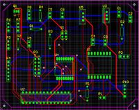
I'm having problems finding out how to tell Altium not to place a via under the pads when auto routing as you can see in the attached picture. Can anyone tell me how I can resolve this?
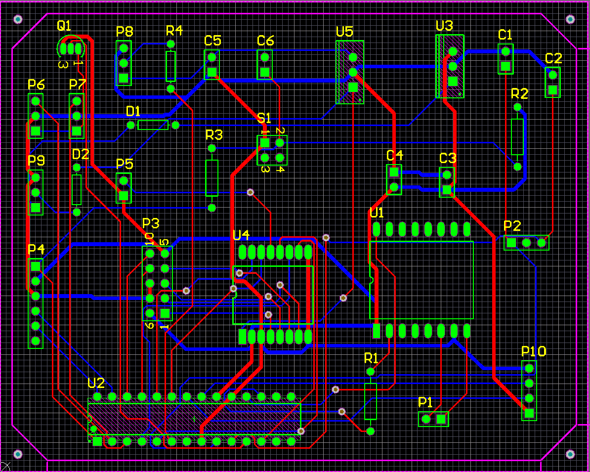
Thank you for your reply. What I'm trying to say is that I will solder the components on the bottom layer so I would like all traces leading to component pads to be on the bottom layer. And I would also prefer all via outside component courtyard if possible.
First of all, do NOT use the autorouter if you don't know how to configure it properly. The layout you'll end up with will be horrible.
Secondly, you'll have to place your components first before you start the routing process; they're too far apart and not placed in a logical order. Take a look at the placement of Q1 as an example of suboptimal placement. Why are the decoupling caps so far away from the ICs? Also keep in mind that connectors must be placed at the edge of the board for optimal accessibility.
This site uses cookies to help personalise content, tailor your experience and to keep you logged in if you register.
By continuing to use this site, you are consenting to our use of cookies.