Continue to Site

Welcome to EDAboard.com

Welcome to our site! EDAboard.com is an international Electronics Discussion Forum focused on EDA software, circuits, schematics, books, theory, papers, asic, pld, 8051, DSP, Network, RF, Analog Design, PCB, Service Manuals... and a whole lot more! To participate you need to register. Registration is free. Click here to register now.

[SOLVED] NEGATIVE LOOP GAIN OF LDO

Status
Not open for further replies.

Arnab1233

Newbie
Joined
Jul 7, 2022
Messages
5
Helped
0
Reputation
0
Reaction score
0
Trophy points
11
Activity points
151
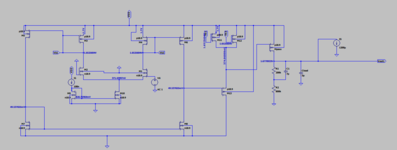
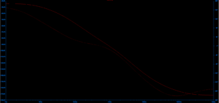
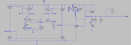
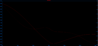
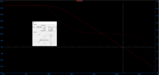
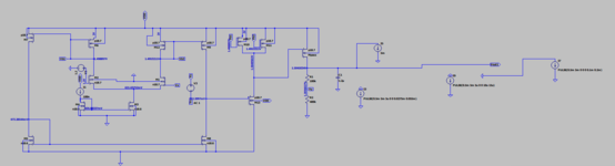
I am trying to design an LDO with the following specification: Vout = 1.5V; Vin = 1.7V - 2V; Iload = 75uA to 1200uA. However, while I am simulating its loop gain, its gain is coming negative. Even though all the transistors are in saturation within the given load condition. I have attached the testbench as well as the Bode Plot for it. Can anybody suggest what might be the reason?
 

Attachments

  • Screenshot 2022-11-25 130817.png
    Screenshot 2022-11-25 130817.png
    22.3 KB · Views: 189
  • Screenshot 2022-11-25 130842.png
    Screenshot 2022-11-25 130842.png
    30.3 KB · Views: 174

Solution
The loop gain measurement needs to be taken at the regular LDO bias point, Vout = 1.5V, Vx = 1.2 V. In the post #3 setup, Vx is still 0V, respectively the amplifier is far from regular bias point. In case the bode plot with about 70 dB loop gain has been made with different bias, you missed to show the respective setup.

I'm unable to foresee how the loop gain with correct bias will look like.
--- Updated ---

You may want to zip and post the LTspice simulation files (.asc and transistor models), we can demonstrate a possible loop gain measurement setup.
Suggest to visualize the operation pints by determing transistor currents and actual gm. Guess you see that the negative gain is just expectable.
The fault is probably zero gate voltage of M1 and M2. Apply correct reference voltage of 1.2 V. With the resulting higher gain, you probably need a real loop gain setup (Middlebrook's method) instead of open loop, or empirical correction of the offset voltage to set expected Vout.
Thank you sir for the insight. I have attached the image for loop gain setup as you recommended. I guess it is a correct setup and the system is fairly unstable due to a very low frequency pole. I will look into the stability matter. However sir I had a question as how the negative gain is expectable?
 

Attachments

  • Screenshot 2022-11-25 151516.png
    Screenshot 2022-11-25 151516.png
    29.7 KB · Views: 138
  • Screenshot 2022-11-25 151530.png
    Screenshot 2022-11-25 151530.png
    29.6 KB · Views: 141

Hi

indeed the log(gain) is negative and thus the dB value is negative,
which means the real gain is somewhere between 0 and 1.

Klaus
 
You might like to check out your testbench with an ideal-ish, known good op amp to be sure that the configuration is right for closed loop.
 
Each circuit with negative feedback must have a negative loop gain due to the sign inversion at the summing node (alternatively: One or three sign inversion at any other place within the feedback loop).
However, this involves the "correct" definition of loop gain.
Unfortunately, two different definitions are in use:

(1) Gain of the complete loop - including the mentioned sign inversion(s). This is what we get when the loop is opened at a suitable node - as it happens during circuit simulation.
In this case, the stability criterion is based on a "critical" phase shift of 360 deg. =0 deg.

(2) Gain of all loop components (product) without the mentioned sign inversion. In this case, the "critical" phase shift is -180deg.
(Comment: To me, the second definition is not a preferrable method because there are systems with (hidden?) phase inversions within the loop. More than that, this method is not compatible with circuit simulations).
 
Last edited:
Hi,

I wanted to point out that the true gain is somewhere between 0 and 1 (positive or negative)
(Indeed the log(negative value) is not defined)

Since the dB value is negative the gain is always below 1.
And if I'm not mistaken a loop is unconditionally stable with a gain < 1. Independent of phase shift.

Klaus
 
The loop gain measurement needs to be taken at the regular LDO bias point, Vout = 1.5V, Vx = 1.2 V. In the post #3 setup, Vx is still 0V, respectively the amplifier is far from regular bias point. In case the bode plot with about 70 dB loop gain has been made with different bias, you missed to show the respective setup.

I'm unable to foresee how the loop gain with correct bias will look like.
--- Updated ---

You may want to zip and post the LTspice simulation files (.asc and transistor models), we can demonstrate a possible loop gain measurement setup.
 
Solution
Thank you all for all the information and suggestion. Indeed as pointed by FvM and KlausST, the problem is with 0 voltage applied at the gate of the input transistors for which the gain drops and falls between 0 and 1, thus giving a negative loop gain. I have also tried the Middlebrooks's Method, as it is more accurate to simulate the closed loop gain. I have attached the images of the testbench as well as the output of the simulation below.
 

Attachments

  • Screenshot 2022-11-29 101418.png
    Screenshot 2022-11-29 101418.png
    45.5 KB · Views: 108
  • Screenshot 2022-11-29 101346.png
    Screenshot 2022-11-29 101346.png
    26.9 KB · Views: 104

Status
Not open for further replies.

Similar threads

Part and Inventory Search

Welcome to EDABoard.com

Sponsor

Back
Top