Continue to Site
Follow along with the video below to see how to install our site as a web app on your home screen.
Note: This feature may not be available in some browsers.
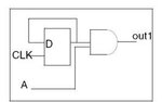
module asg1(d, clk, a, out1);
input d, a, clk;
reg q;
output out1;
reg out1;
wire d = q;
always@(posedge clk)
begin
q <= d;
end
always@(a or q)
begin
out1 = (q & a);
end
endmodule
always@(posedge clk)
begin
q = q;
end


assign d = q;
always@(posedge clk)
begin
q <= d;
endalways@(posedge clk)
begin
q <= q;
endmodule sub_asg1 (clk, a, d, q, out1);
input clk, a, d;
output q, out1;
always @ (posedge clk) q <= d;
assign out1 = q & a;
endmodulemodue asg1 (clk, a, out1);
input clk, a;
output out1;
sub_asg1 i0 (.clk(clk), .d(q), .q(q), .a(a), out1(out1));
endmodule