Continue to Site

Welcome to EDAboard.com

Welcome to our site! EDAboard.com is an international Electronics Discussion Forum focused on EDA software, circuits, schematics, books, theory, papers, asic, pld, 8051, DSP, Network, RF, Analog Design, PCB, Service Manuals... and a whole lot more! To participate you need to register. Registration is free. Click here to register now.

Need some LNA and PA design materials

Status
Not open for further replies.

mahadevsarkar

Newbie level 5
Joined
Feb 25, 2009
Messages
9
Helped
0
Reputation
0
Reaction score
0
Trophy points
1,281
Activity points
1,358
LNA DESIGNING

Respected manjunatha,

since last month i have been trying to design an LNA . can you please help me by sending me LNA and PA design material where step by step every thing is explained. i need your kind help my mail id is mahadevsarkar@gmail.com
please.

regards
sarkar.
 

Re: LNA DESIGNING

I don't mean to be critical but I'm sure this question has been asked around 1496 times in this very forum (I know I just exaggerate the number). There is a top right most corner box at the main index of this forum with the word SEARCH next to it. You should type something like LNA or LNA AND DESIGN to see if it comes up with something interesting.

FYI, This fellow Manjunatha_hv had posted a lot of tutorial materials for LNA here. You may search for his post related with his name. Another poster named Boy also has 2 LNA tutorials very good for beginner.
 

Re: LNA DESIGNING

Hello sarkar,


The procedure for LNA Design from Specifications all depends upon implementation of the LNA & the Method or EDA tool used...

Say for example for MMIC LNA design & Hybrid MIC LNA some of the steps differs...
Again the availability of the model S-parameters or Nonlinaer spice model...

Start with the the device analysis, such as Stability, input,output reflection coefficient measurements, Gain, Noise Figure then choose the Stable network for the device if unstable...

Then if it is non linear device Bias the deice using biasing netork (if S-parameters no need since it is measured data at perticular bias conditions)...

Then finally build the matching network from input to get better Noise, & Gain...
Plot all other measurements such as VSWR, Impedance, etc...
Build the layout & export it as DXF or Gerber...

---manju---
 

Re: LNA DESIGNING

Respected manjunatha,

i have been designing and developing LNA for Mobile and defence(800MHzt o 6.0 GHz) bands for TMA project i took a packaged/ chip transistor.
it's absolutely correct while changing bands, topology of the design must be changing. but i think the concept of the design will remain unchanged only realization will be differed from frequeccy to frequency. as an example i must realise inductance in lumped fastion at lower frequency but same inductance i must realise in distributed fastion when my frequency of operation is much higher, i think i am correct. my request was to you about the procedure, not on realization. actually i started few days back even i don't know the right way to start designing. in this web page i saw you helped to lot of persons. so my kind request is if you don't mind please send me some document about the procedure of LNA designing in that above mentioned band.

thanking you for your kind suggestion in your reply.
 

Re: LNA DESIGNING

Hello Sarakar,

you can call me manju...

The procedure for designing for the band first choose the device from vendors such as AVAGO, NEC, NXP, Infineon, etc...based on cost performance, availability
of model & device...

Then use the CAD (EDA) software for simulation & analysis such as Microwave Office (MWO) or ADS...


---manju---
 

LNA DESIGNING

13_1239393026.jpg


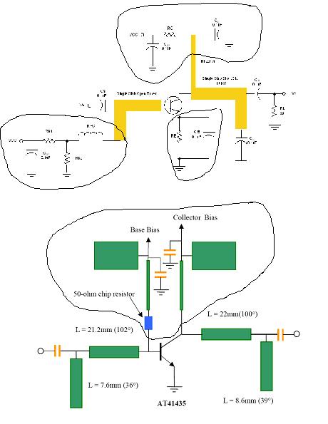
hii manju I have attached a jpg whic is a LNA can you help me how to do the biasing calculation for this

rgds
jagath
 

LNA DESIGNING

what i want help on is,I have done the i/p and o/p matching network for LNA microwave amplifier,but how do you bias the transistor?
is it that you have to doo a separate normal ciruit for biasing and supply the voltage to the microstrip circuit through wires or do i use lumped components and design a bising circuil in the microstrip board it self can some one help me with this

rgds
jagath
 

Re: LNA DESIGNING

well if u using ADS it's very easy to design a bias circuit for the BJT as it has an inbuilt function that will do that,,,,and since the bias circuit is a DC circuit u will b ok if u use resistors for the biasing...the only thing is u need to provide a ground or short circuit to the RF signal in the bias network...a very common way of doing that would be to use a quarter wavelength high impedance line followed by an open stub...the open stub could be a radial stub for a better bandwidth performance...this colud be followed by another quarter wave high impedance line and an open stub of required....then u can provide the bias voltages across this..hope this helps...
 

Re: LNA DESIGNING

it's my earnest request regarding designing------------
Can you help me to get or can please provide me Les Besser's vedio materials for amplifier( LNA and Power) designing.

i feel i will be helped.

thank you in advance
SARKAR
 

Status
Not open for further replies.

Part and Inventory Search

Welcome to EDABoard.com

Sponsor

Back
Top