Continue to Site

Welcome to EDAboard.com

Welcome to our site! EDAboard.com is an international Electronics Discussion Forum focused on EDA software, circuits, schematics, books, theory, papers, asic, pld, 8051, DSP, Network, RF, Analog Design, PCB, Service Manuals... and a whole lot more! To participate you need to register. Registration is free. Click here to register now.

Need help on my thesis regarding insertion loss of my PA design

Status
Not open for further replies.

Wall-eee

Newbie level 6
Newbie level 6
Joined
May 26, 2013
Messages
11
Helped
0
Reputation
0
Reaction score
0
Trophy points
1,281
Visit site
Activity points
1,388
i'm currently working on my masters thesis where i have to design and implement a broadband UHF 50W Class AB PA single ended.
i was able to determine the optimum load and source impedance using loadpull simulations..my Zopt= 2 - j1.8

i'm now into my matching network designs at the input and output for my 50-ohm load and 50-ohm source. i'm using a 4 section LC network in this configuration.

using ideal LC parts, i get very good insertion and return losses (RL< -10, IL > -0.1)..then i progressively chance into real LC parts models (from ATC) then to changing inductor to transmission lines. the Insertion loss response are still acceptable but degraded to around -0.5dB for the whole UHF band.

next i did a schematic (input matching network) to connect all the real LC parts with MLIN (from MWO) and configure such that it is close to my desired layout...using the closed form models and LC models, my IL response becomes very bad even after optimization. it is now in IL ~ -1.8dB..

i then tried to do Extraction in MWO (EM simulation) and even getting worse which is quite expected based.

i'm quite worried because when i go to output matching and i get this range of insertion losses, then my PA efficiency is very problematic..

any advise on my thesis problem?
 

Not very clear for me, but from my understanding when you look at the output IL of the PA this is about -0.5dB, and when you do the input match of the PA, the output IL loss goes to -1.8dB.
One thing that have to take into account is that the simulator is adding also the Mismatch Loss which is: ML(dB) = 10*LOG(1-Γ²)
When do the input matching, the PA output impedance is changing (due to the PA isolation) so the output return loss (and mismatch loss) is changing.
The best thing that can help you, is to do a input/output Load-Pull to find the best compromise between input and output PA matching.
 
"when you do the input match of the PA, the output IL loss goes to -1.8dB."

I would like to know if the above is true because if you did the load pull for input and output simultaneously the output match loss would not be affected by the input match in this way. This assumes you are not comparing small signal performance to your large signal load pull analysis.

If the 1.8dB is input matching circuit loss and 0.5dB on the output then the impact on efficiency is less significant.

Either way, to reduce loss consider using a better and/or thicker board material for distributed inductors or use some high Q wire wound inductors from coilcraft.

You could examine the possibility of using less sections in your matching circuits.

Edit: when you analyze the insertion loss are you changing the port impedance to reflect the device's impedance? You must not use a 50 ohm port for the device's side of the circuit.
 
Last edited:
Not very clear for me, but from my understanding when you look at the output IL of the PA this is about -0.5dB, and when you do the input match of the PA, the output IL loss goes to -1.8dB.
One thing that have to take into account is that the simulator is adding also the Mismatch Loss which is: ML(dB) = 10*LOG(1-Γ²)
When do the input matching, the PA output impedance is changing (due to the PA isolation) so the output return loss (and mismatch loss) is changing.
The best thing that can help you, is to do a input/output Load-Pull to find the best compromise between input and output PA matching.

i'm sorry if my topic is not clear...the insertion losses above are just for the passive matching networks. the PA is not included in the simulations yet but I just did load pull and source pull which i then used to design my matching networks.
my problem is that i'm having to high Insertion losses for the matching networks alone.

From loadpull: Zopt=1.5 - j 1.6 -----> i used Z*opt for my matching [ lp-lp-lp-hp topology]
From sourcpull: Zopt=1.5 - j0.2 ----> i also used conjugate of Z*opt for my source matching [ hp-lp-lp-lp topology]

- - - Updated - - -

"when you do the input match of the PA, the output IL loss goes to -1.8dB."

I would like to know if the above is true because if you did the load pull for input and output simultaneously the output match loss would not be affected by the input match in this way. This assumes you are not comparing small signal performance to your large signal load pull analysis.

If the 1.8dB is input matching circuit loss and 0.5dB on the output then the impact on efficiency is less significant.

Either way, to reduce loss consider using a better and/or thicker board material for distributed inductors or use some high Q wire wound inductors from coilcraft.

You could examine the possibility of using less sections in your matching circuits.

Edit: when you analyze the insertion loss are you changing the port impedance to reflect the device's impedance? You must not use a 50 ohm port for the device's side of the circuit.


i'm sorry if my topic is not clear...the insertion losses above are just for the passive matching networks. the PA is not included in the simulations yet but I just did load pull and source pull which i then used to design my matching networks.
my problem is that i'm having to high Insertion losses for the matching networks alone.

yes i changed my port to PORTG to reflect the conjugate optimum impedance of my source and loadpulls...my problem when reducing the section is my BW is affected since i need 470-860M.

From loadpull: Zopt=1.5 - j 1.6 -----> i used Z*opt for my matching [ lp-lp-lp-hp topology]
From sourcpull: Zopt=1.5 - j0.2 ----> i also used conjugate of Z*opt for my source matching [ hp-lp-lp-lp topology]
 

Sourcepull impedance is pretty strange.That's why-perhaps-IL is very high due to high transformation ratio..
While you amplifier is terminated with its Optimum Load Impedance, what range of Optimum Source Impedance you have found ??
 
Sourcepull impedance is pretty strange.That's why-perhaps-IL is very high due to high transformation ratio..
While you amplifier is terminated with its Optimum Load Impedance, what range of Optimum Source Impedance you have found ??

oops my mistake...i interchanged my optimum impedance for load and source...my source is 1.5-j1.6...my load is 1.5 - j0.2

by the way, these load and source pulls are based from my 2-tone loadpull simulations....

would you recommend using 1-tone load and source pull isntead?
 
Last edited:

because you are trying to match to an impedance so close to the outside of the smith chart, you are destined to have errors! Simulation errors, implementation errors, component Q related errors. you simply can not go from 50 ohms to such a small impedance without those errors adding up.

So, for a thesis, you should be able to defend why such errors exists. I suggest you study the bilinear transform as it relates to the smith chart.

Another think, you should attempt to empirically improve the performance in the lab. It is one thing to know how to simulate, it is a whole other and better thing to figure out how to actually succeed.
 
oops my mistake...i interchanged my optimum impedance for load and source...my source is 1.5-j1.6...my load is 1.5 - j0.2

by the way, these load and source pulls are based from my 2-tone loadpull simulations....

would you recommend using 1-tone load and source pull isntead?

It's still strange.This impedance is too low ( whatever type of transistor you used-bipolar or FET) for a source and matching will cost you by huge insertion loss.
The first thing you should do is to find Optimum Load Impedance with a single tone while the input is driven with 50 Ohm standard impedance.
In this case check your Gain,Output Power,Efficieny, etc.Then do the same thing with 2-tones to check IM performance.
I mean, optimize the output first for ALL case and then play around Source Impedance that is less effective on PA performance.

according to the manufacturer of this LDMOS, they even have around 1.6 - j 1.4 optimum load impedance for P3dB but their bias setting is different from what i have used so it is quite close...

my design process actually started from 1-tone to determine my max. output power and efficiency compromise...afterwhich i performed source pull using the derived optimum load impedance...i then get my sourcepull for my optimum and compromised set of gain, pout and efficiency.....

next i performed 2-tone (using the same average input power) and found out that at the same bias settings, the optimum loadpulls for power, efficiency, gain quite differs from 1-tone results....

since 2-tone is more representative of my real input signal, i focused on 2-tone loadpull and sourcepull to determine a compromised optimum impedanbce for my required power and IMD.


could this be a model issue of the transistor?
as you said, maybe i need to use 1-tone results instead....

i will let you know my results...
 

according to the manufacturer of this LDMOS, they even have around 1.6 - j 1.4 optimum load impedance for P3dB
i will let you know my results...

Optimum Load Impedance is OK but Source Impedance is too low.
That's why you got high Insertion Loss at the Input due to high transformation ratio
 

It's still strange.This impedance is too low ( whatever type of transistor you used-bipolar or FET) for a source and matching will cost you by huge insertion loss.
The first thing you should do is to find Optimum Load Impedance with a single tone while the input is driven with 50 Ohm standard impedance.
In this case check your Gain,Output Power,Efficieny, etc.Then do the same thing with 2-tones to check IM performance.
I mean, optimize the output first for ALL case and then play around Source Impedance that is less effective on PA performance.

just a clarification below statement;

"find Optimum Load Impedance with a single tone while the input is driven with 50 Ohm standard impedance"

if i understand it correctly, you mean just input a 50-ohm 1Tone power source with an ideal Bias Tee at the gate and then at the output use a Load Tuner?

what i did initially is to also put a source tuner with initial gamma equal to the conjugate of of S11. after doing the loadpull, i will then use its optimum Z and then generate my source pull...
i have not yet tried just inputting a standard 50 ohm source..
 

Sourcepull impedance is pretty strange.That's why-perhaps-IL is very high due to high transformation ratio..
While you amplifier is terminated with its Optimum Load Impedance, what range of Optimum Source Impedance you have found ??

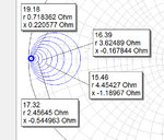
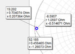
shown below are the sourcepull for Gain and large signal S11, using an optimum load impadance derived from max. P1dB loadpull

sourcepull Large Signal S11.jpgsourcepull PGain.jpg

another plot below shows the sourcepull optimum impedances for Gain, S11 large signal and Pout, while using the optimum load impedance @ P1dB

zopts.jpg
 
Last edited:

Optimum Load Impedance is OK but Source Impedance is too low.
That's why you got high Insertion Loss at the Input due to high transformation ratio


If you use a push-pull configuration you could reduce the transformation ratio. The impedance transformation ratio of the balun is often 2:1 so the matching circuit can be simplified. ie. Matching from a 25-ohm source to a 1.6-ohm load vs a 50-ohm source to a 1.6-ohm load is easier.
 

If you use a push-pull configuration you could reduce the transformation ratio. The impedance transformation ratio of the balun is often 2:1 so the matching circuit can be simplified. ie. Matching from a 25-ohm source to a 1.6-ohm load vs a 50-ohm source to a 1.6-ohm load is easier.

this is good solution but my thesis requires just a single ended configuration because my thesis includes cost.
 

this is good solution but my thesis requires just a single ended configuration because my thesis includes cost.

Push pull could allow you to meet your requirement with a lower power therefore less costly device. However, I don't know if that would be enough to offset the cost of a second device.
I wish you luck.

Joel
 

Status
Not open for further replies.

Part and Inventory Search

Welcome to EDABoard.com

Sponsor

Back
Top