Continue to Site

Welcome to EDAboard.com

Welcome to our site! EDAboard.com is an international Electronics Discussion Forum focused on EDA software, circuits, schematics, books, theory, papers, asic, pld, 8051, DSP, Network, RF, Analog Design, PCB, Service Manuals... and a whole lot more! To participate you need to register. Registration is free. Click here to register now.

Need help on getting the desired specs of my schematic.

Status
Not open for further replies.
I have not used a MOS capacitor and don't know how it works and whether it needs any other bias, etc.

Bandwidth will drop with miller compensation. That is expected. One option is increasing the tail current in the first stage. This gives higher gm for the input pair and pushes out the UGB. Also add the series resistance like I have said before as this will improve phase margin. with these two handles you can optimize for better BW.
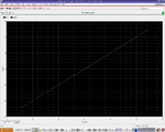
 

DCSimulation.png
This is the dc simulation after i change the test bench, this is wrong right??
 

if you see that your gain is small as you said (when it become as the input), then may be you have a large offset voltage. it is very important to simulate the input offset voltage

Im not sure if i can make another new circuit, need to ask my teacher since she told me to modify the circuit the circuit to meet specs. im doing a assignment.

- - - Updated - - -

Ehh i changed the test bench, i did get a better gain, but BW n PM seems to become worst, and my dc simulation become a straight line, the same as input

- - - Updated - - -

if you see that your gain is small as you said (when it become as the input), then may be you have a large offset voltage. it is very important to simulate the input offset voltage

Im not sure if i can make another new circuit, need to ask my teacher since she told me to modify the circuit the circuit to meet specs. im doing a assignment.

- - - Updated - - -

Ehh i changed the test bench, i did get a better gain, but BW n PM seems to become worst, and my dc simulation become a straight line, the same as input
 

Sweep from -2.5v to 2.5v at 0.1v step size
n i dun realli need higher gain as i already met the specs of minimum 60db, now main thing is to get BW n PM
 

Try this out. This is from the Allen Notes. Use the same circuit that you have.


  1. Fix you tail current of the first stage. This was probably the one given by your teacher.
  2. Size the tail current transistor accordingly.
  3. Your Load Capacitor is 1pF, Select Compensation capacitance as 0.2pF
  4. Fix the Gm of the input pair from the equation UGB = gm/Cc. Select a suitable UGB and fix gm.
  5. Get W/L for the input pair from the above gm using the formula relating gm, Id and W/L.
  6. Set the W/L for the PMOS current mirror load as double the size of the NMOS input pair. (This can be changed later.)
  7. Set the sizes for the second stage using the balance condition
    (W/L)PM3 / (W/L)PM5 = 2 * (W/L)NM5 / (W/L)NM3
    I have used the names of transistors from your circuit.
  8. You have the ratio of the sizes for the second stage. Size them according to the current you want.
  9. Apply Vdd and Vss, Set inputs to zero and run dc operating point simulation and check if everything is in saturation.
  10. Run ac simulation using the new test bench. If possible use C = 1F and R = 1000Meg
  11. This should give you a preliminary design. Now you can start tinkering around the sizes and currents to tune your circuit.
  12. If not satisfied with the PM, add a zero right before UGB. To do this insert a Resistor in series with your compensation capacitance. the value of the resistor should be from the equation UGB = 1/RcCc.
  13. Start with minimum Lengths for all transistors. If not satisfied with the gain, increase the lengths in the first stage. Scale widths also accordingly.
 
  • Like
Reactions: DualX

    DualX

    Points: 2
    Helpful Answer Positive Rating
Waa thx nitishn5! i will try it, hopefully will get the specs! :) and thanks soo much for ur help.

- - - Updated - - -

Ehh i cant figure out how to get KN' and Kp' etc.. in the lecture note u asked me to read, is there a way to calculate or do i hav to make up the values myself?
btw i need to get BW of 35Mhz, so gm=35Mhz X 0.2p X 2pi?
 

To get Kp and Kn, do the Id vs Vgs and Id vs Vds chara on a NMOS and a PMOS device with W/L to be say 3µ/0.5µ.
Use the relations and equations to get Kn/Kp. Do this for different points (Id/Vds/Vgs) and check if the result from each of the is close by.

This should have been the first thing to be done. You cannot start a design without knowing any of the process numbers involved.

Yes you need to to do the 2*pi thing for it. All are in radians/sec.
 

Ohh okay, how do i get the values of Id, Vgs, Vds? btw all these are derived through calculations right? no need to use computer to simulate anything yet?
 

1. Do a dc operating point simulation of a NMOS and PMOS with Vgs = 1V and Vds = 1.8V
2. Find out Id and Vth of both transistors from the operating point
3. Use the equation Id = 0.5µnCox(W/L)(Vgs - Vth)2 and calculate µnCox
4. Try this out for different values of W/L, Vgs and Vds.
5. With more values you can also find out λ (Channel length modulation parameter).
6. If you are interested, you can plot the Id vs Vgs curve by doing a dc sweep. You can then use curve fitting techniques to find out what is the whether the square law holds true. I have seen that for L = 0.18µm, the equation has a power of 1.32. You may not have to worry about this since you are using bigger lengths.
7. With the values of Kn and Kp in hand, do the procedure I gave you before.
 
  • Like
Reactions: DualX

    DualX

    Points: 2
    Helpful Answer Positive Rating
ok thanks, will try it out :)
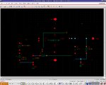
Btw the dc simulation is still abit weird, am i putting the connections correct?
TestBench.png
 

Your Connections look ok.

What do you mean your DC simulation looks weird?
Dude, you need to stop giving vague replies like the one above. Just show what all you are seeing and then we can try to sort it out.

Btw, I hope you click the helped me buttons in this whole thread!!
 

I still get jus 1 line for the output during dc simulation, swept from -2.5 to 2.5v. pic is above
 

1. Do a dc operating point simulation of a NMOS and PMOS with Vgs = 1V and Vds = 1.8V
2. Find out Id and Vth of both transistors from the operating point
3. Use the equation Id = 0.5µnCox(W/L)(Vgs - Vth)2 and calculate µnCox
4. Try this out for different values of W/L, Vgs and Vds.
5. With more values you can also find out λ (Channel length modulation parameter).
6. If you are interested, you can plot the Id vs Vgs curve by doing a dc sweep. You can then use curve fitting techniques to find out what is the whether the square law holds true. I have seen that for L = 0.18µm, the equation has a power of 1.32. You may not have to worry about this since you are using bigger lengths.
7. With the values of Kn and Kp in hand, do the procedure I gave you before.

Sry but i dont really understand how to do the 1st step, how do i do the connections n on which component to change the values? And 2nd step, where do i hav to measure to get those values? Sry n thanks for ur help!
 
Last edited:

I had assumed you had done a Id-Vds and Id-Vgs charaterestics plotting in you course.

Take an NMOS. Connect a voltage source between Gate and Source (Vgs) and another voltage source between Drain and Source (Vds). Ground the Source Terminal. Set tha voltages that I have give above. For PMOS set negative voltages. Run a DC operating point Analysis, This will be there as part of the spice simulator that you are using,
It will give a dc Operating point solution which contains all the info about the circuit. It will have all info about each transistor like gm ,gds, Vth, capacitances etc. It would probably be saved in a file. You might have to ask some senior in the lab to know where to find it.
Use this information.

I feel that you don't know how to use the Virtuoso Analog Design Environment yet. You might want to go through some basic simulations on that before jumping straight onto Opamp Design.
 
  • Like
Reactions: DualX

    DualX

    Points: 2
    Helpful Answer Positive Rating
Ehh i get it now, i did the simulation before, just didnt know theres a name for that hahas. okay i will try out the steps now, will post again if i come across anymore problems, thank you very much nitishn5!
 

Status
Not open for further replies.

Part and Inventory Search

Welcome to EDABoard.com

Sponsor

Back
Top