Continue to Site

Welcome to EDAboard.com

Welcome to our site! EDAboard.com is an international Electronics Discussion Forum focused on EDA software, circuits, schematics, books, theory, papers, asic, pld, 8051, DSP, Network, RF, Analog Design, PCB, Service Manuals... and a whole lot more! To participate you need to register. Registration is free. Click here to register now.

Need help on getting the desired specs of my schematic.

Status
Not open for further replies.

DualX

Junior Member level 1
Joined
Dec 9, 2012
Messages
17
Helped
0
Reputation
0
Reaction score
0
Trophy points
1,281
Activity points
1,404
Really need help on meeting the specifications on my circuit, the specs to meet are >1kV gain(60db), phase margin of 40-80degree and bandwidth of 35Mhz. The biggest problem is still getting the bandwidth and PM, as for the gain i've managed to get above 1kV. Please help me! Would really appreciate any help!! Thanks in advance!
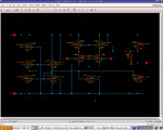
Schematic.pngSimulationCircuit.pngWaveform.png
Initial(specs).pngScaling(specs).png
 
Last edited:

Hi,

You can increase the Compensation capacitance to improve the phase margin, at the cost of Bandwidth.
You can increase the gm of the input pair by using larger W or increasing the current and increase the bandwidth since for miller compensated 2 stage opamp, UGB = gm/Cc.

If you can provide the db plot for gain and also the phase plot it would give a better ideas on the location of the poles.
 

The pole formed at the output of the second stage has to be outside the unity loop gain frequency. Loop gain, please note, is the product of the opamp gain with the feedback factor. Now, the output pole will be approximately situated at gm2/CL. gm2 is the transconductance of the second stage. CL is load capacitance. Find out the load capacitance and then find out the required gm2 to keep the output pole outside the unity loop gain frequency. Usually, noise specification will set your first stage transconductance. Based on this, you can choose the compensation capacitor.
 

Actually there is another problem, i understand that changing the value of Cc should affect the phase margin and bandwidth, but it's not functioning like how it supposed to be, everything stays the same when i change the values, at most a fee degrees of difference for the PM, is there any other ways to increase bandwidth n PM? Thanks alot for helping btw!

- - - Updated - - -

Oh n btw im using nmoscap1v3 becoz there is a symbol for creating the layout later on, the normal capacitor don't hav a symbol, but when i put bac the standard capacitor for the circuit, it doesnt work anymore, not sure if it does affect or not
 

Your test bench is wrong. Without feedback , dc operating point of the output stage will not be set in your opamp. Running a dc or or ac analysis will not be meaningful without proper dc negative feedback. You may refer to Chapter 6 of Allen Holberg ,section Measurement and simulation of opamps.
 

Ehh sry but i dont realli understand, could u jus point out what i need to do? sry for the trouble, im realli new at this x.x and thanks!
 

What is your vdd and vss values?
 

Your test bench is wrong. Without feedback , dc operating point of the output stage will not be set in your op-amp. Running a dc or or ac analysis will not be meaningful without proper dc negative feedback. You may refer to Chapter 6 of Allen Holberg ,section Measurement and simulation of op-amps.

I dot think feedback is necessary for a single ended output op-amps.

@DualX
what monsoon means is that you should give a resistor feedback like you give in regular discrete op-amps and then do the simulations.

You can go through the following for a step by step design procedure.
**broken link removed**
and Allen's (of Allen, Holberg) lecture notes.
**broken link removed**

These do not give proper explanations for the selecting some of the values but you can solve those by hand yourself. The other lecture notes by Allen are quite good and can be kept as a reference for design of op-amps.
 

I dot think feedback is necessary for a single ended output op-amps.
In the architecture given by DualX it is needed. You can convince yourself by seeing that the dc voltage of Vout is not properly defined in the open loop. To measure the open loop characteristic you should use something like as shown in the attachment. Chose a very high value of R and C.
 

Attachments

  • simu.pdf
    133.4 KB · Views: 163

Im using 2.5v for vdd and -2.5v for vss. thx monsoon n nitishn5, i'll take a look at the lectures notes :) btw i did scaling of all transistor lenght/2 and width x2, my gains dropped to 100v but PM and BW both increased, now i hav 15° PM n 10Mhz, i onli fear that the BW will decrease after i change the transistor size to increade gain. I will post the initial specs n the specs after scaling later
 

@monsoon

I guess you are right. My bad.

@DualX

Do not arbitrarily scale like this.
In your original design, try increasing the width of the nmos input pair and then double its length(scale W also). You can also reduce the pmos W a bit. This would give you a good gain. I dont know why you have set such a big W for your second stage pmos.
Set your Cc to be 0.2 times your Load cap.

And try the test bench with the circuit given by monsoon. Use huge R and C.

BTW why have you given a 1.85mV dc bias to one of your inputs in your original test bench??
 
Last edited:

That is to make Vout close to 0, this voltage source is set to the input offset voltage so that if no other signal is present, the output voltage will be approximately 0
 

@nitishn5
tried the method, gain did improve but not the PM and BW, as for the test bench, why is there + & - on vdd n vss?? If i just connect vdd n vss to gnd then there will be a error. Im not realli sure on how to connect them. Sry for the trouble! I know its hard trying to help me since i don't know quite alot of stuffs, but i realli appreciate the help guys! Thanks again!
 

In your Test bench, connect R between vout ans vm and connect C between vm and ground. keep the rest the same.
Set R to be 100Megaohms and set C to be around 10uF.

I think your RHP Zero is screwing your phase margin. You can insert a resistor in series with your compensation cap to put the zero to the LHP. You might find the theory textbooks in the chapter related to frequency compensation. Place the Zero right before the UGB and you will get 45 degrees additional PM at UGB.
 

I highly recommend you to consider the design procedure of the two stage Op-amp from chapter 6 by Allen Holberg, just folllow it. this procedure is assured to have optimum phase margin of around 60 by putting the second pole so far from the GBW. second thing, I think if you would use a normal capacittor rather than MOS capacitor you will get better result


Really need help on meeting the specifications on my circuit, the specs to meet are >1kV gain(60db), phase margin of 40-80degree and bandwidth of 35Mhz. The biggest problem is still getting the bandwidth and PM, as for the gain i've managed to get above 1kV. Please help me! Would really appreciate any help!! Thanks in advance!
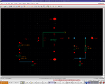
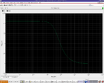
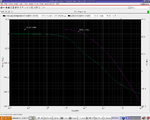
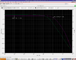
View attachment 84189View attachment 84190View attachment 84191
View attachment 84262View attachment 84263
 

@nitishn5
ok thx i will try it out tml, can onli do in sch using sch com with the program installed.

@Junus2012
i am supposed to get this circuit to meet the specs, i cant just make a new 1 >.< but i will take a look at the designs guide, and as for y i used MOS capacitor is becoz there is a symbol for use in the layout, whereas the normal capacitor dont. Thanks btw! :)
 

why cant you do new one, two stage Op-amp is the very simple to construct and you have ready procedure for it from Holberg

@nitishn5
ok thx i will try it out tml, can onli do in sch using sch com with the program installed.

@Junus2012
i am supposed to get this circuit to meet the specs, i cant just make a new 1 >.< but i will take a look at the designs guide, and as for y i used MOS capacitor is becoz there is a symbol for use in the layout, whereas the normal capacitor dont. Thanks btw! :)
 

Im not sure if i can make another new circuit, need to ask my teacher since she told me to modify the circuit the circuit to meet specs. im doing a assignment.

- - - Updated - - -

Ehh i changed the test bench, i did get a better gain, but BW n PM seems to become worst, and my dc simulation become a straight line, the same as input
 

Can you give the value of the compensation capacitance that you are using? If you can, try it wit a regular capacitance instead of a mos capacitance. Check if your library has a thing called 'mimcap'. If so try with that also.

Have you done RC compensation? Add an R in series to your compensation. Get the value from 1/RcCc = 2*pi*UGB.

If both don't work you can go through the design procedure in Allen Holberg or the lecture notes I posted before. You can use the existing circuit. The design procedure is not circuit dependent, it will just give you the values for the diff pair and the like.
 

Im using 300f but it can be changed, dont know y this capacitor value dont affects the PM n BW no matter how i change the value. N yes there is mimcap, shld i put it under capacitance/length/width? and what values shld i put? thanks!

- - - Updated - - -

Tried out the mimcap, finally the capacitor statts to function like how it suppose to, but the BW dropped by alot even when i put capacitance to 17.6f(width 4u, length 4u) the smallest capacitance allowed, theBW is lower than compared to using MOS capacitor
 

Status
Not open for further replies.

Part and Inventory Search

Welcome to EDABoard.com

Sponsor

Back
Top