Continue to Site

Welcome to EDAboard.com

Welcome to our site! EDAboard.com is an international Electronics Discussion Forum focused on EDA software, circuits, schematics, books, theory, papers, asic, pld, 8051, DSP, Network, RF, Analog Design, PCB, Service Manuals... and a whole lot more! To participate you need to register. Registration is free. Click here to register now.

Need Explanation (Zero Crossing Detector)

Status
Not open for further replies.

ArdyNT

Full Member level 2
Full Member level 2
Joined
Nov 6, 2012
Messages
126
Helped
7
Reputation
14
Reaction score
7
Trophy points
1,298
Visit site
Activity points
2,304
I just start to build zero crossing detection circuit. I'm using center tap transformer to reduce 220 V AC source.
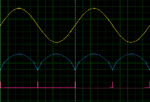
and here is the screen shoot:

ZCD.png

OSC.png

First, is that circuit correct?

Second, can anybody explain how this circuit works? (completely)

Third, when I remove D4, I got nothing (the blue and red in oscilloscope is still a straight line), do you know WHY ?


Thank you very much.
 

Hi,

The circuit looks OK, I don't know what you exactly what you want.

The transformer and the diodes D1 and D2 form a full wave rectifier whose output is the waveform in blue.
The capacitors and the 7805 forms a regulated voltage supply. The capacitors filter out ac components and stores the charge. The reason you have 2 capacitors in parallel is because one is a electrolytic capacitor( a better capacitor at low freq) and the other is a ceramic capacitor (better at higher freq).
If you plot the waveform at the input of the 7805 you would get a sawtooth type waveform typical of a Capacitor Filter Fullwave rectifier circuit. This is the waveform you would see if you remove D4 (you say it is a straight line but you need to zoom in quite a bit since your capacitors are huge and you have no load.)

The 7805 gives 5V output which is used to drive the LED and also to power the zero crossing detector.

The zero crossing detector here is a transistor which is switched ON and OFF. When the input goes high, the transistor turns ON and its output (collector) turns low. Th collector resistor and the base resistor limits the current through the device. When the input goes low(lower than Vbe of transistor) the transistor turns OFF and since there is no current through the collector, the output is pulled up to 5V (given by the 7805). Since the input to your zero crossing detector is the full wave rectified output(blue) which goes low for a very short time, you see spikes at the output of you detector(red).

When you remove the Diode D4, the input to your zero crossing detector is the sawtooth waveform described before. Since it is always high that is why the red is a straight line.
 

Status
Not open for further replies.

Similar threads

Part and Inventory Search

Welcome to EDABoard.com

Sponsor

Back
Top