alexan_e
Administrator
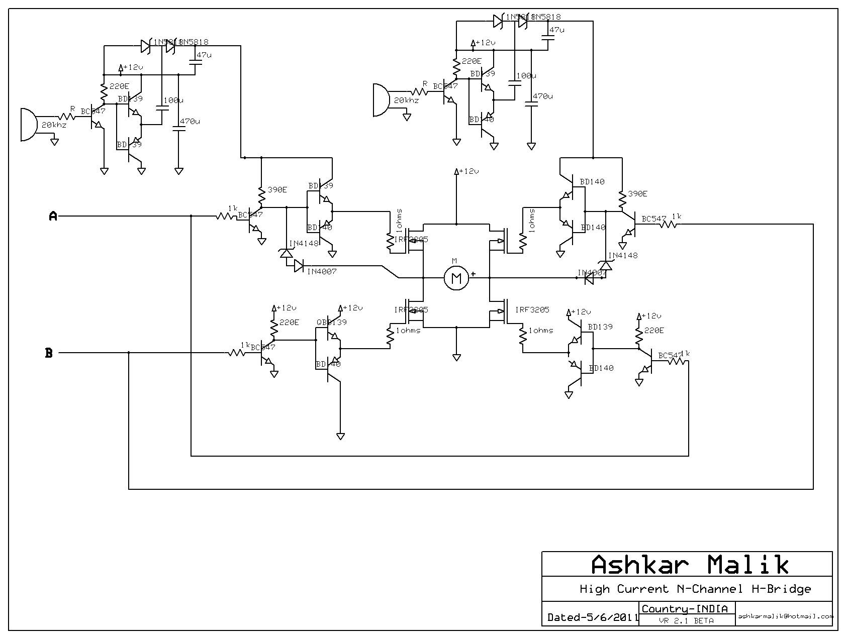
from http://obrazki.elektroda.pl/77_1307291856.jpg
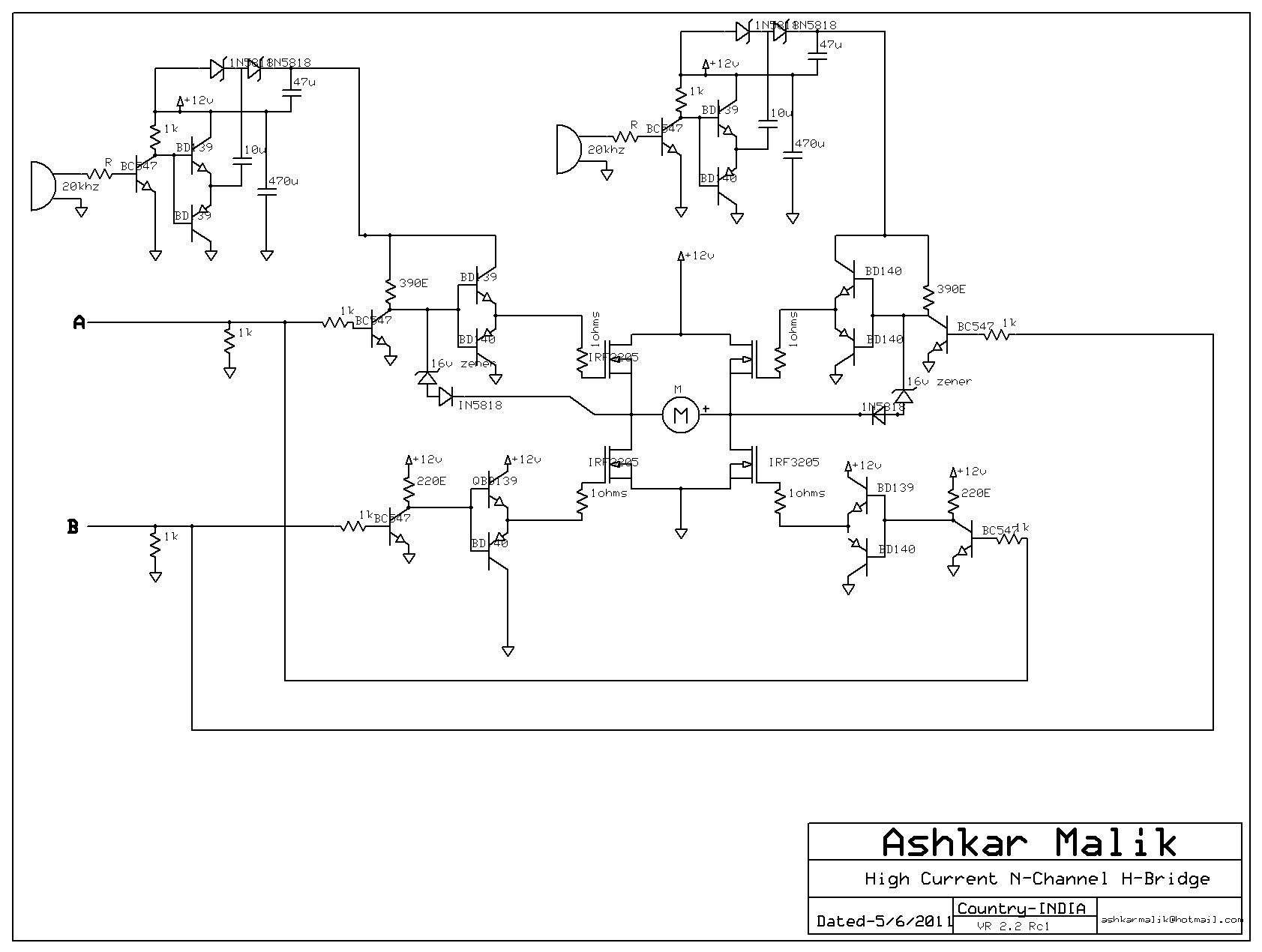
reverse both diodes , then zener cathode (the triangle tip) goes to the BC547 collector and the diode cathode goes to the source pin of the mosfet.
**broken link removed**
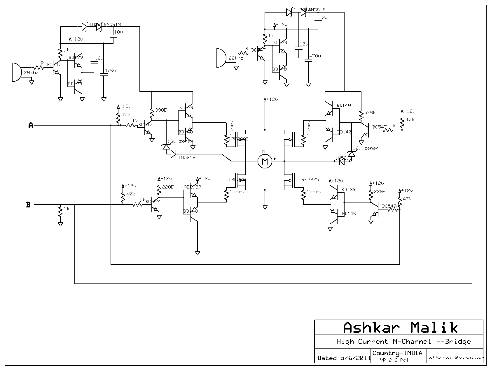
reverse both diodes , then zener cathode (the triangle tip) goes to the BC547 collector and the diode cathode goes to the source pin of the mosfet.
**broken link removed**
")
