Continue to Site

Welcome to EDAboard.com

Welcome to our site! EDAboard.com is an international Electronics Discussion Forum focused on EDA software, circuits, schematics, books, theory, papers, asic, pld, 8051, DSP, Network, RF, Analog Design, PCB, Service Manuals... and a whole lot more! To participate you need to register. Registration is free. Click here to register now.

my sample&hold circuit takes a lot of time to arrive at steady state

Status
Not open for further replies.

mohamis288

Full Member level 3
Full Member level 3
Joined
Mar 1, 2022
Messages
165
Helped
0
Reputation
0
Reaction score
1
Trophy points
18
Activity points
1,233
Hello,

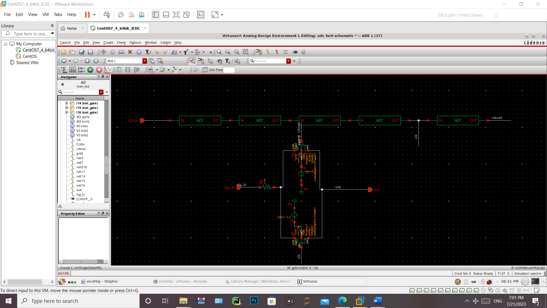
part of ADC is a Sample&Hold circuit. here is the circuit of my simple S&H circuit:
Screenshot (942).png


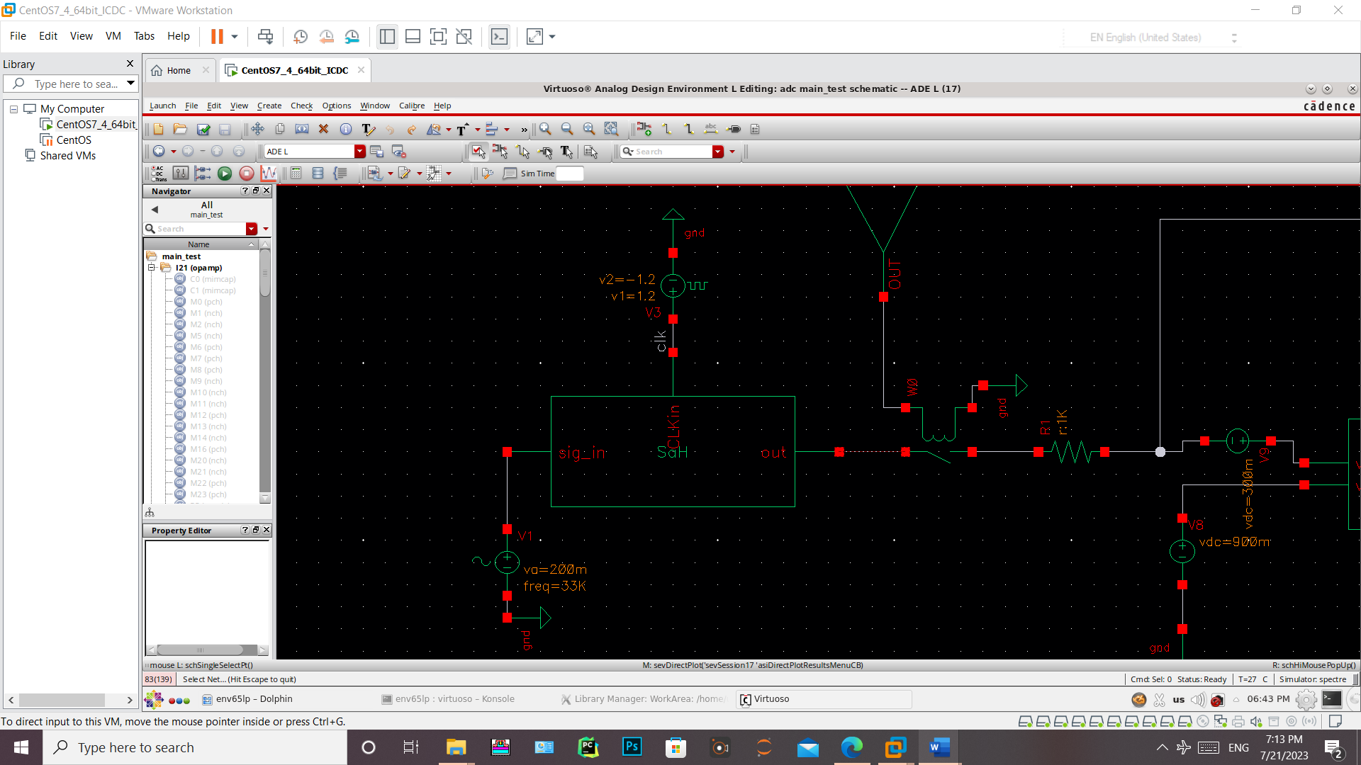
its symbol in the original circuit is shown in the following:
Screenshot (944).png


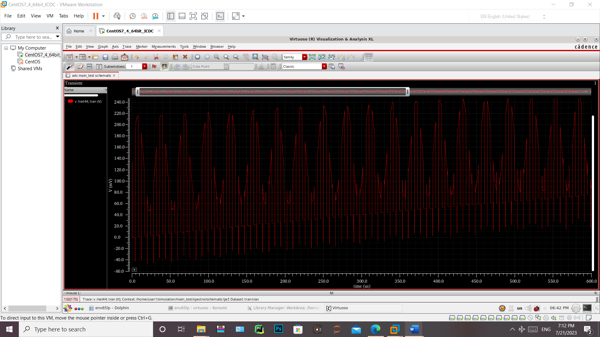
input signal is a 33KHz 200m volt sinusoidal wave with DC level of 300m V. sampling frequency is about 4 times of input frequency. it is used in a dual slope ADC. as shown below, output voltage of S&H circuit is in the transient state. it takes a lot of time to arrive at steady state, what can I do to overcome this problem?
Screenshot (943).png
 

Solution
Where is your "hold" capacitor?

Without it, all you'll see is toggling and the switching charge on
turnoff (absent from your ideal switch model) will determine the
(alleged) "hold" voltage.

Hard full scale gate drive will give you a common mode dependent
sample pedestal voltage. Imbalance in Cdg (and if high Zin, Cgs) will
give you a charge offset too.

Put a layout-realistic hold capacitor on the output and resimulate.
Look at close-in port currents at the sample-to-hold edge for
charge imbalance and resulting pedestal.
 

Solution
Status
Not open for further replies.

Part and Inventory Search

Welcome to EDABoard.com

Sponsor

Back
Top