shawnmirror
Newbie level 1

- Joined
- Aug 15, 2013
- Messages
- 1
- Helped
- 0
- Reputation
- 0
- Reaction score
- 0
- Trophy points
- 1
- Activity points
- 10

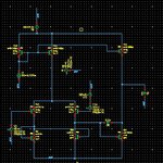
Dear all, I now design a two stage opamp,as the first photo, the tran simulation of the first stage output the differential input and second stage output are shown in the second photo, why the second stage tran simulation results is like this one? I thinl it's wrong, but i don't know why. the AC gain and phase are shown in the third photo, the gain can't drop to 0, what is the reason?

![A(CH26(GU]336UK5[%]OREW.jpg A(CH26(GU]336UK5[%]OREW.jpg](https://www.edaboard.com/data/attachments/35/35249-d6b337113996e9d58692ed64fa2cd5f2.jpg)
I know I should use xfmr to build the differential input, the connection is like

but can someone tell me, why I get error when do the simulation"unexpected voltage source/inductor loop, including `lmk1'
" I connected the circuit like

who can tell me the left bottom pin should connect to where?
