Continue to Site

Welcome to EDAboard.com

Welcome to our site! EDAboard.com is an international Electronics Discussion Forum focused on EDA software, circuits, schematics, books, theory, papers, asic, pld, 8051, DSP, Network, RF, Analog Design, PCB, Service Manuals... and a whole lot more! To participate you need to register. Registration is free. Click here to register now.

[Moved]MOSFET Inverter Oscillator

Status
Not open for further replies.

electronZ

Member level 2
Member level 2
Joined
Apr 11, 2010
Messages
43
Helped
0
Reputation
0
Reaction score
0
Trophy points
1,286
Visit site
Activity points
1,602
MosOsci.png

Hi all,

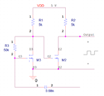
I found this circuit without explanation. I am able to have square wave at the output. I think I understand how this circuit works, but I know that I don´t have all the details.

When 5V gets applied at Drain om M3 (D3), M2 will turn on. This will result in current flowing into D2, and the output will be low, as it is connected to ground.

At the same time, current starts to run through R1 and R3 charging up the capacitor on pin 1. After some time, the voltage at capacitor pin 1 will reach Vth of M3. This will result in M3 gets turned on, current starts to flow through D3, causing M2 to turn off, since its gate is now connected to ground.

However, if someone can help me find an expression of the frequency the circuit can generate, and explain why R3 should be around 10 times R1 - I have been told that it will ease the calculations, cause then I only have to worry about R3*C - I will be grateful
Or just general description of the operation, maybe more details. Does anyone have any sources I can read about this circuit?


thank you.
 

The frequency depends on how long it takes for the capacitor to charge to the threshold voltage of the Mosfet. The charging time is simply R in ohms times C in Farads, and is in seconds. One cycle is one charge time plus one discharge time.

The problem is that the frequency will be inaccurate due to the range of the threshold voltage of a Mosfet. Maybe you should measure the threshold voltage.

R3 must be a high value so that the charge time is almost the same as the discharge time.
 

I´m not sure if took a suitable MOSFET model, but it seems in the simulation as output period does not exactly match will constant RC time of circuit components, is that correct ?

image.JPG
 

... output period does not exactly match will constant RC time of circuit components, is that correct ?

R3 is in a negative feedBack path. So the actual toggle time interval doesn't depend on RC and the MOSFET's threshold voltage only, but will be prolonged by the feedBack via R3, too.
 
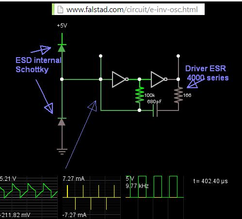
The Falstad Cmos oscillator is not the "classic" one I post here.
The classic one does not need external diodes because they are built-into Cmos logic as protection diodes. An additional resistor is added in series with the input to isolate the capacitor from being affected by the diodes.
 

Attachments

  • Cmos oscillator.png
    Cmos oscillator.png
    101.6 KB · Views: 95

Thanks for all the inputs, guys. Appreciated.

I have been calculating, simulating and I will construct it today.

But a silly question:
The capacitor charges up to Vth of M3, and it gets turned on. This results in having a high at the output - 5 V at pin 2 on capacitor. The voltage at pin 1 on the capacitor jumps to around 5.5 V.
Why? - i would say the capacitor do not like the sudden change in the voltage across it so it is compensating the change on pin 2, but again how would the calculations look like?

Plot:
SuddenChangeCap.png

thanks guys...
 

If you used CMOS output instead of a drain R on NMOS, you would get a 5V step above threshold or >7V and then a negative step to -3V.

But with CMOS input , it would be peaks at 7.5, -2.5, decaying to +2.5V, but as I showed, the internal Schottky diodes clamp it to one diode drop outside the rails. In my case +\-0.21

Hi Sunny,

Thanks, but am not sure I understand. Care to explain, please?
 

Status
Not open for further replies.

Similar threads

Part and Inventory Search

Welcome to EDABoard.com

Sponsor

Back
Top