Continue to Site

Welcome to EDAboard.com

Welcome to our site! EDAboard.com is an international Electronics Discussion Forum focused on EDA software, circuits, schematics, books, theory, papers, asic, pld, 8051, DSP, Network, RF, Analog Design, PCB, Service Manuals... and a whole lot more! To participate you need to register. Registration is free. Click here to register now.

MOSFET saturation in diff amp design

Status
Not open for further replies.

OG_

Newbie level 6
Joined
Jun 11, 2019
Messages
11
Helped
0
Reputation
0
Reaction score
0
Trophy points
1
Activity points
198
Hello,

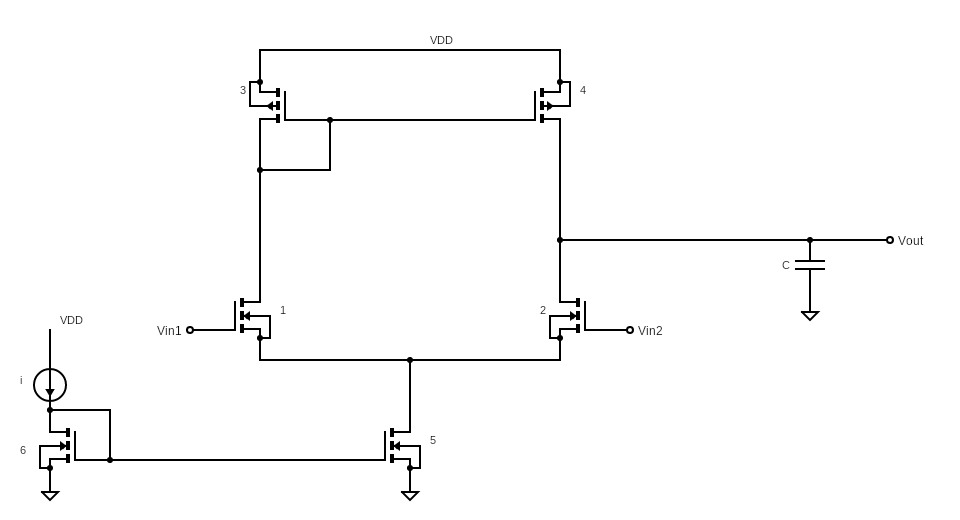
I am designing a diff amp in cadence virtuoso with the following architecture:
1625510475386.png


I am new to designing these amplifiers, so I started with noise/power constraints and worked my way from there. At the end of the day, I have the perfect AC response, gain is great, noise specs and power constraints are satisfied, AND it works across my input DC operating range. However, I performed a DC analysis around the bias points of my circuit that I was using on all previous analysis and I see none of the transistors are in saturation. In fact, some are even in the "0" range (which means cutoff according to this:https://community.cadence.com/cadence_technology_forums/f/custom-ic-design/14626/operating-region).

For a week I drove myself crazy trying to get the transistors in saturation, but inevitably, that would ruin one of the constraints I had.

My main question is this:
1. Based on this info, does it seem like one of my previous analysis were done incorrectly?
2. In industry, is it common to achieve all transistors in saturation in a diff amp design using 1.8V and super low power?
3. If transistors are not in saturation, what is something I should be super careful of/aware of? I think the main issue of not having transistors in saturation is that there would be non linearities based on the bias points.

Thank you! Let me know if you'd like any clarifications
 

Sometimes you don't get to do what the textbook
says is ideal. Like when your supply headroom is
not much more than VT. And some positions just
will not allow operation in saturation regime by
topology.

It's a place to start, trying to optimize device OP.
It's not a criterion for acceptance of the design -
exhaustive proof of spec table compliance, is that.
 

This structure can have high gain and to ensure proper operating point it has to work with negative feedback. Did you applied feedback?
 

This structure can have high gain and to ensure proper operating point it has to work with negative feedback. Did you applied feedback?
My signals are on the scale of microvolts, and in the open loop configuration I have a voltage gain of ~40 db to my bandwidth (~10KHz). I know it is weird using open loop, but the absolute gain can vary a decent amount before I would saturate my output. I have a lot of constraints for this application because it is fairly niche so having a varying gain is alright as long as long as I can calibrate it initially to derive the gain. Do you think it would change significantly over time? I know it feels wrong making this open loop, but it appears to work so far (extensive sims, of course different from reality which is why I am asking about it here).
 

If you have microvolt-range signal then be sure to pay
attention to simulator DC and transient accuracy settings.
You'll pay a price in solution time, but better than getting
a solution which is more about numerical noise than the
circuit response.

But without closed loop operation, there's a likelihood
that your amplifier at input differential = 0.0000000000V
imposed, is one side or the other from true null, and gain
will fall away fast as you depart from VID=Vio.
 

But without closed loop operation, there's a likelihood
that your amplifier at input differential = 0.0000000000V
imposed, is one side or the other from true null, and gain
will fall away fast as you depart from VID=Vio.

Can you elaborate on what you mean by this? Thank you for the response!
 

In case of ideal transistors (ideally flat output characteristic) , in open loop configuration the output voltage is indefinite. In case of real devices, the output voltage can be whatever between the rails.

If you need 40dB gain amplifier, design >40dB opamp and close the loop with 100/1 resistor ratio. Or you will need another amplifier to set common mode level.
 

My signals are on the scale of microvolts, and in the open loop configuration I have a voltage gain of ~40 db to my bandwidth (~10KHz). I know it is weird using open loop, but the absolute gain can vary a decent amount before I would saturate my output. I have a lot of constraints for this application because it is fairly niche so having a varying gain is alright as long as long as I can calibrate it initially to derive the gain. Do you think it would change significantly over time? I know it feels wrong making this open loop, but it appears to work so far (extensive sims, of course different from reality which is why I am asking about it here).
I think you misunderstood Dominiks point.

In your answer you assume that you have a microvolt input which would then generate 100 microvolt output. But what about all other effects? What happens if you have an input referred offset of 10 mV? Some kind of feedback is required.

If you started with ac and noise, and didn't look at the DC point. How do you know that the output wasn't around 0 V all the time?

Back to your actual question. No, it's not a problem to have transistors in another region than saturation but you should be aware of the pros and cons. For example matching tends to decrease when running in subthreshold.

Also for your design process, don't look at the region. Look at the vdsat and veff, the region might say saturation but if you're 1 mV from triode or subthreshold you will end up there over PVT and mismatch. I don't remember the critiera for region 0 but it's even more off than region 3, subthreshold, and I'm sure you have a problem somewhere.

Perhaps you could annotate the DC point and share that image? Both with transistor OP points and node voltages.
 

Status
Not open for further replies.

Similar threads

Part and Inventory Search

Welcome to EDABoard.com

Sponsor

Back
Top