Continue to Site

Welcome to EDAboard.com

Welcome to our site! EDAboard.com is an international Electronics Discussion Forum focused on EDA software, circuits, schematics, books, theory, papers, asic, pld, 8051, DSP, Network, RF, Analog Design, PCB, Service Manuals... and a whole lot more! To participate you need to register. Registration is free. Click here to register now.

MMZ09332B NXP power amplifier

Do you know the difference between "Power Gain" and "S21 ?
1699995179098.png

More information
 
I am self-taught in the field and I don't know everything. can you explain to me very simply how to understand this and how to interpret it on the datasheet please
 
S-parameters are measured with the device with a 50 ohm source and load. The data sheet gives the performance with matching circuits between the device and 50 ohms, hence the increased gain.
 
Did you use 13 db using 10 * log (s21) is power gain from s-parms?

Does NXP use voltage gain or power gain for s21 (dB) ?
1700001830232.png


If I assume NXP's file for s21 is voltage gain then I used 20*log (s21)
1700001457329.png

- old ref on discussing this...
 
Last edited:
S-parameters are measured with the device with a 50 ohm source and load. The data sheet gives the performance with matching circuits between the device and 50 ohms, hence the increased gain.
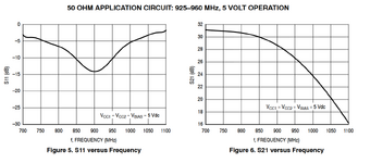
Exactly. From the 50 Ohm S-parameters we can see that the "raw" transistor is poorly matched to 50 Ohm.
We really need additional matching network to get the maximum available gain.

"Raw" S-parameters in 50 Ohm environment, with no matching circuit:

MMZ09332B_SP.png


Maximum available gain when matched:

MMZ09332B_Gmax.png
 
this would therefore mean that the S parameter file was measured directly on the pins of the component and in the datasheet we have the S parameter measurements with a matching circuit according to the frequencies used? is it correct?
what is confusing for me is how to interpret these two curves in the attachment. nxp not giving their measurement condition.
I put my component on a layout and I measured with a VNA and I got the same results as their S parameter file
 

Attachments

  • S21_MMZ09332B.PNG
    S21_MMZ09332B.PNG
    47.4 KB · Views: 52
  • S21_MMZ09332B_21.PNG
    S21_MMZ09332B_21.PNG
    70.5 KB · Views: 65
this would therefore mean that the S parameter file was measured directly on the pins of the component and in the datasheet we have the S parameter measurements with a matching circuit according to the frequencies used? is it correct?
Yes, correct.

what is confusing for me is how to interpret these two curves in the attachment. nxp not giving their measurement condition.
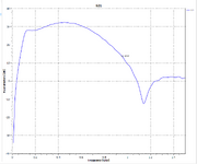
The second curve that you show is for a matched amplifier. In the data sheet the circuit and layout are shown together with that curve.
 
i do not see this S-parameter file in the OP post, so i can not discuss in detail.
but you do realize that S parameters of a semiconductor device are UNMATCHED. i.e. you take the semiconductor chip, and measure the input and output ports on a 50 ohm network analyzer.

so if the Sparameters say X gain in a 50 ohm system, and then you ADD an input matching network and an output matching network, you can reduce the input and output return losses, and that will make the apparent gain be much higher.
 

LaTeX Commands Quick-Menu:

Part and Inventory Search

Welcome to EDABoard.com

Sponsor

Back
Top