Continue to Site

Welcome to EDAboard.com

Welcome to our site! EDAboard.com is an international Electronics Discussion Forum focused on EDA software, circuits, schematics, books, theory, papers, asic, pld, 8051, DSP, Network, RF, Analog Design, PCB, Service Manuals... and a whole lot more! To participate you need to register. Registration is free. Click here to register now.

mm-wave inductor modeling in hfss

Status
Not open for further replies.

natnoraa

Full Member level 1
Full Member level 1
Joined
Jun 19, 2011
Messages
98
Helped
12
Reputation
24
Reaction score
11
Trophy points
1,288
Visit site
Activity points
2,108
Hi guys,

I know this could be a question in analog IC layout but since it's for rf/mm-wave domain, am thus seeking some advice here.

I have a rfline model from a pdk and from the process file, i see that it consists of the top most metal layer and a silicon substrate. Say I'm using a line of 100um and i find that the layout it's just a straight drawing of that 100um and it's too large.
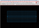
rfline.png

I would like to draw and simulate something like (it is a simplified sketch and the width is 4um):

line.png

1) can i do a drawing from cadence virtuoso layout suite and then export to hfss?
2) do i have to draw the return path (i assume it will be layer M1) in cadence or only when am simulating in HFSS?
3) do i have to use any vias (m1 all the way to the top most layer) to connect return path all the way to top most metal layer or they will be floating?
4) the path i've drawn, i assume both layers will be exactly identical and from the 3d point of view, the top most metal layer will just be on top of the bottom layer?
5) what's the gap in between the 2 layers we're looking at? foundry's limitation and process?
6) will the return path contribute to losses?
7) the layout generated from virtuoso will be exactly identical to what i've simulated in circuit simulation but not so from hfss?
8) after hfss simulation is done i'll export it back to cadence virtuoso?

If there's any guide you can point me to I will be glad to listen and learn. Thanks in advance!

Constraints: i only have a layer mapping tech file and amat files foundry provided for hfss. i can't simulate the components in hfss. only in cadence.

Natnoraa
 
Last edited:

1) yes.
2) i'm not familiar with cadence, but you can draw it in HFSS.
3) for microstrip no vias needed. if stripline, then you should have vias connecting top and bottom ground planes
4) return path should be solid ground plane on bottom layer if possible.
5) I'm not sure on internal layer thicknesses, but silicon chips can be as small as 2 mils thick overall.
6) yes. especially if you are meandering a narrow ground line rather than using a ground plane.
7) not sure what you are asking.
8) exporting simulation or geometry? both can be done.
 
Hi reidintransit,

3) i was actually being told that i have three pins for GSG. G pins are connected all the way to the bottom plate (i chose M2) through the vias. S pin will be drawn the same layer as i've used for the signal path. Is this right? If so, what are the two G pins for in the case as shown? to provide a return path? return path for? I do not want to continue working on it without having a deeper understanding.
ind.png

4) noted. thanks :)
7) please ignore this question
8) say after drawing in cadence, i export the gds to hfss and run em simulation. thereafter i adjust the length of the strip until i get the required inductance identical to the one i simulated in cadence, then i export geometry or simulation back to cadence to simulate with the main circuit?

Thanks for your time in reading and providing your insight.

Natnoraa
 

3) GSG is ground signal ground which is what you would use if you were creating a standalone circuit that you want to be able to measure with probes or if you need to connect the ground from this object to another (like a separate circuit board) with ribbons or wirebonds.
4) Q3d from Ansys is better for extracting inductance values. From HFSS you can export S-parameters or an equivalent circuit model which should be able to go back into cadence for electrical simulation in cadence.
What frequency range are you looking at for this?
 

Hi reidintransit,

3) i understand that it's the ground signal ground for a standalone circuit. Intuitively, a ground and a signal pin should suffice but why do we need two ground pins and furthermore at both input and output ports like what i've drawn?

4) Sadly, I do not have access to Q3d but only hfss em simulator. I've heard a lot about being able to export it back. Need to find out how to :) Am looking at 60GHz.

P.S: Apologies for the late reply

Natnoraa
 
Last edited:

Hi again reidintransit or anyone as a matter of fact,

to build on what you've advised, attached is a crop of the design:
hfss.png

1) The signal trace is the top metal, which is also the inductor am drawing. is it correct to draw two rectangle 'tapes' at the two ends and excite them to be port 1 and 2?

2) the ground plane i was advised to use m2. someone said to draw it as large as possible. but why? and how large is large? for now, i've drawn it from cadence to be about the size that can encompass the signal trace metal line. typically the ground we'll assign 'pec' material to it but since my ground is now the metal layer m2, am still assigning the metal layer to it. anything wrong with it? am using m2 as my reference for the 2 ports.

3) if i expand the ground plane m2, i can expand the airbox and all the dielectric layers am i right?

4) after validating and running the simulation, I would want the inductance i can get from the purple trace metal. it's terminal driven for the lumped ports. What I want is the series inductance between the two ports? the formula is Zseries = -2/(Y(port1,port2)+Y(port2,port1)) and then Ls = im(Zseries)/(2*pi*f). is that right? because what am getting from the results is showing me about 3nH whereas the same length in cadence is about 76pH. the difference is too huge?

P.S: I just saw the formula for finding inductance from it would be ind = im(1/Y11)/(2*pi*f)

results.png

Natnoraa
 
Last edited:

When working with frequencies as high as 60GHz Coplanar Waveguide gives cleaner fields than just GS. Many of the probes used to test such structures use probes that are ground signal ground (GSG) so it helps to have that configuration.
4) Right click on your setup, select Matrix Data. there are buttons for exporting S-parameters or equivalent circuit on that tab.
 

Status
Not open for further replies.

Part and Inventory Search

Welcome to EDABoard.com

Sponsor

Back
Top