MahmoudHassan
Full Member level 6

- Joined
- Oct 4, 2010
- Messages
- 349
- Helped
- 44
- Reputation
- 90
- Reaction score
- 40
- Trophy points
- 1,328
- Activity points
- 3,919
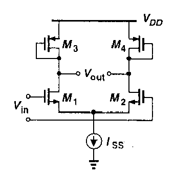
For the Circuit shown in figure 1 it is required to know the minimum allowable output voltage

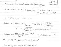
for fig 2 it is the instructor solution for it

as there is two constraints or possibility
the first one M1 at the edge of triode region
and so vout1,2 Min = Vss + VDS1 and as m1 at the edge of triode region VDS1 = VGS1-Vthn so Voutmin can be calculated
the other possibility (the one i am not understand )
When all of ISS pass through M3 when this can happen and why this may happen ?
the first and second constraint solution is shown in fig 2
(This problem number is 4.14 in Design of Analog CMOS integrated circuti by B.Razavi page 130 and solution in page 107 in instructors solution manual )

for fig 2 it is the instructor solution for it

as there is two constraints or possibility
the first one M1 at the edge of triode region
and so vout1,2 Min = Vss + VDS1 and as m1 at the edge of triode region VDS1 = VGS1-Vthn so Voutmin can be calculated
the other possibility (the one i am not understand )
When all of ISS pass through M3 when this can happen and why this may happen ?
the first and second constraint solution is shown in fig 2
(This problem number is 4.14 in Design of Analog CMOS integrated circuti by B.Razavi page 130 and solution in page 107 in instructors solution manual )
