Continue to Site

Welcome to EDAboard.com

Welcome to our site! EDAboard.com is an international Electronics Discussion Forum focused on EDA software, circuits, schematics, books, theory, papers, asic, pld, 8051, DSP, Network, RF, Analog Design, PCB, Service Manuals... and a whole lot more! To participate you need to register. Registration is free. Click here to register now.

microstrip line inductance decreasing

Status
Not open for further replies.

yefj

Advanced Member level 5
Joined
Sep 12, 2019
Messages
1,502
Helped
1
Reputation
2
Reaction score
5
Trophy points
38
Activity points
9,092
Hello, If we have a complex long and curved trace and we get problematic insertion loss.
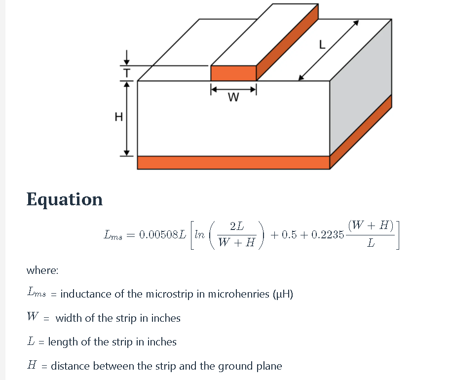
Is the thickness of the trace place a role in the inductance of transmition line?
by the formula bellow its not
And in general what is the general method of improving insertion loss in microstrip trace?
Thanks.
1615312520996.png
 

Thickness of the trace may not have much influence on the microstrip inductance, but impedance of the trace and its consistency during entire length may play an important role when is about insertion loss.
You mentioned you have a curved trace. A curved trace has minimum parasitic inductance and capacitance (so minimum insertion loss) only when the curving radius is larger than twice of the width of the line.
 

So assume i have a proble with insertion loss in such trace ,how i fix it?
Thanks.
 

Your emphasis on inductance and inductance reduction seems inappropriate. The first point for transmission performance is designing it with matched impedance and keeping the impedance constant along the line. Secondly you have dielectric und resistive losses according to the transmission line geometry and material properties.

It would be helpful to understand what your transmission application and exact design problem is.
 
Hello FVM,i am trying to learn this issue.
Suppose you did simulation and design but in manufatoring it resulted not as you simulated.
How you fix it?
Thanks.
 

Transmission line impedance can vary due to 1. substrate permittivity variation, 2. substrate thickness variation, 3. etching process variations.

The usual way is to adjust the photo mask line width or the etching process according to impedance measurements. (impedance controlled manufacturing).
 
  • Like
Reactions: yefj

    yefj

    Points: 2
    Helpful Answer Positive Rating
Insertion loss is influenced by metal loss and dielectric loss. If you have a lossy substrate like FR4, substrate losses (loss tangent) have a large effect on line insertion loss.
 
  • Like
Reactions: yefj

    yefj

    Points: 2
    Helpful Answer Positive Rating
Status
Not open for further replies.

Part and Inventory Search

Welcome to EDABoard.com

Sponsor

Back
Top