jose_peeterson
Newbie level 6
Dear all,
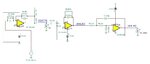
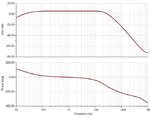
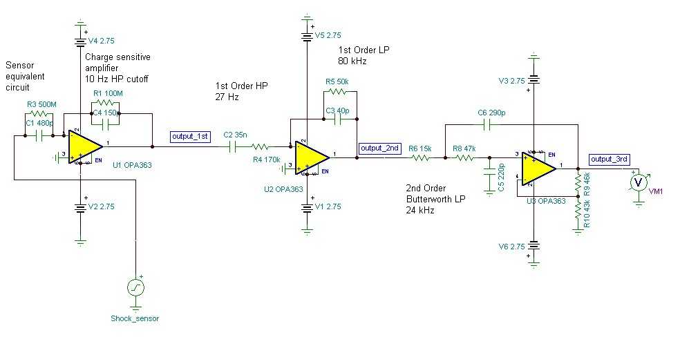
I am using "TINA ti" to design a shock sensor circuit. The sensor is represented by a "ac source with a capacitor in series and a resistor in parallel". The aim is to design the circuit with signal conditioning to allow only signals in the frequency range 300 to 20khz.
I think the amplitude of the "ac source" represents the "g forces of shock". so the device should be able to measure 5G to 500G without clipping the op-amps rails.
First, I did not use any method but just randomly insert cap and resistor values to meet the frequency criteria. the reference circuit is here https://www.datasheets.org.uk/PKGS-00NB-R_PKGS-00NB-R/Datasheet-077/DSAE0057787.html
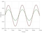
Now the transient analysis is not as expected. for even 1mv i get clipping. I have to change back the cap and resistor values which in turn affect my frequency response.
Can somebody please help me how to build the 3 stages separately and put them together.
please view my circuit and the values to comment on this.
Thanks,
SS_3_STAGES_COMPLETE.JPG
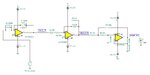
I am using "TINA ti" to design a shock sensor circuit. The sensor is represented by a "ac source with a capacitor in series and a resistor in parallel". The aim is to design the circuit with signal conditioning to allow only signals in the frequency range 300 to 20khz.
I think the amplitude of the "ac source" represents the "g forces of shock". so the device should be able to measure 5G to 500G without clipping the op-amps rails.
First, I did not use any method but just randomly insert cap and resistor values to meet the frequency criteria. the reference circuit is here https://www.datasheets.org.uk/PKGS-00NB-R_PKGS-00NB-R/Datasheet-077/DSAE0057787.html
Now the transient analysis is not as expected. for even 1mv i get clipping. I have to change back the cap and resistor values which in turn affect my frequency response.
Can somebody please help me how to build the 3 stages separately and put them together.
please view my circuit and the values to comment on this.
Thanks,
SS_3_STAGES_COMPLETE.JPG