Continue to Site

Welcome to EDAboard.com

Welcome to our site! EDAboard.com is an international Electronics Discussion Forum focused on EDA software, circuits, schematics, books, theory, papers, asic, pld, 8051, DSP, Network, RF, Analog Design, PCB, Service Manuals... and a whole lot more! To participate you need to register. Registration is free. Click here to register now.

Measuring S-parameters of RF Power Amplifier

Status
Not open for further replies.

Mabrok

Full Member level 4
Joined
Mar 1, 2017
Messages
223
Helped
0
Reputation
0
Reaction score
1
Trophy points
18
Activity points
1,597
Dear All,

please I need your help and advise upon the following:

I have designed and fabricated PA, during the simulation the results was very good. During the measurements using VNA "Keysight E5071C model", I got unexpected S22 (almost 0 dB), and also S21 (below 0 dB). For S11 I think it is acceptable which just shifted by 500 MHz to the high frequency.

Additional information which may help:

Target frequency band: 3.4-3.6 GHz
I have used an external attenuator of 30 dB
During measurements, I just performed 2 port calibration and connected the device to the ports of VNA and applied bias.
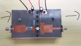
I have attached the photo of the fabricated device and simulation (red) versus measurements (blue) results.

Thanks in advanced
 

Attachments

  • S-parameters sim Vs Measurements.png
    S-parameters sim Vs Measurements.png
    19.2 KB · Views: 335
  • Fabricated device.jpg
    Fabricated device.jpg
    2.1 MB · Views: 272

Your layout is not appropriate. Especially decoupling capacitors are not tied by screws. The screws which are used for Emitter/Source pins are anodized and they are definitely not proper for RF.
There is not via for GND connections.. etc etc..
So, please review your layout carefully..
I post here a good example..
1635078485654.png
 

    Mabrok

    Points: 2
    Helpful Answer Positive Rating
It doesn't have to be double-sided like the Cree example, but the dielectric and ground plane must be like your simulation tested with tolerances.

Retest, and notice any sensitivity in your results when applying pressure to BOT layer to metal substrate using dry wood or plastic rod pushed down around signal track. This may affect parasitic inductance of gnd plane. Also use Phase plots and Smith chart to analyze.

The effective Dk and gap of signal to gnd are critical factors when affected by parasitic inductance variations of gnd plane. (L/C)

Noitce this example in open top layer but proximity to gnd
1635081539283.png
 
Last edited:

I have used an external attenuator of 30 dB

With the 30dB attenuator at the output of you amplifier, you cannot measure amplifier S22.

If you calibrate without attentuator, you will measure almost no reflection from DUT because of the attenuator in between. And if you try to calibrate with attenuator in place, total reflection from cal standards will be attenuated by 2*30dB, which is too much for calibration to work.

So it is expected that S22 isn't meaningful using attenuator.
 

    Mabrok

    Points: 2
    Helpful Answer Positive Rating
The SMA connections in and out do not look like 50 ohms to me, there does not appear to be any track under connector pins. You also do not appear to have any DC blocking capacitors, not a problem if the VNA is DC blocked, but what about the attenautor?
 

Looks like there are small (0402 or so) blocking capacitors next to the connectors. Not so good in terms of impedance matching but at least capacitors.

It's not clear how the VNA has been calibrated considering the 30 dB attenuator. Volker already mentioned that it's almost impossible to get meaningful s22 measurement through attenuator, but how's the gain calibration?


With the 30dB attenuator at the output of you amplifier, you cannot measure amplifier S22.

If you calibrate without attentuator, you will measure almost no reflection from DUT because of the attenuator in between. And if you try to calibrate with attenuator in place, total reflection from cal standards will be attenuated by 2*30dB, which is too much for calibration to work.

So it is expected that S22 isn't meaningful using attenuator.
So, that means I have to remove the attenuator and measure again?
--- Updated ---

Looks like there are small (0402 or so) blocking capacitors next to the connectors. Not so good in terms of impedance matching but at least capacitors.

It's not clear how the VNA has been calibrated considering the 30 dB attenuator. Volker already mentioned that it's almost impossible to get meaningful s22 measurement through attenuator, but how's the gain calibration?
I also have used external DC block "Agilent 11742A Blocking Capacitor"
--- Updated ---

With the 30dB attenuator at the output of you amplifier, you cannot measure amplifier S22.

If you calibrate without attentuator, you will measure almost no reflection from DUT because of the attenuator in between. And if you try to calibrate with attenuator in place, total reflection from cal standards will be attenuated by 2*30dB, which is too much for calibration to work.

So it is expected that S22 isn't meaningful using attenuator.
How about S21?
 
Last edited:

Attenuator is used to protect the VNA against input signals above the damage level (26 dBm for E5071C) which can be easily produced by the power amplifier output. It has to be included in two-port through calibration.

Measuring S22 (or even S11) of a power amplifier is somewhat risky. You need to double check before that the amplifier isn't oscillating.

Agilent shows how to test DUT with Directional couplers and attenuators for testing all s parameters
The diagram shows the internal design of the VNA. The couplers are already there when using an industry standard VNA like E5071C.
 

    Mabrok

    Points: 2
    Helpful Answer Positive Rating
Attenuator is used to protect the VNA against input signals above the damage level (26 dBm for E5071C) which can be easily produced by the power amplifier output. It has to be included in two-port through calibration.

Measuring S22 (or even S11) of a power amplifier is somewhat risky. You need to double check before that the amplifier isn't oscillating.


The diagram shows the internal design of the VNA. The couplers are already there when using an industry standard VNA like E5071C.
Already checked the oscillation with signal generator and spectrum analyzer over wide frequency range and did not observe any oscillations.
 

I think that you have to see first in your measurements why the S21 (gain) is below 0dB.
Whatever minor mistakes on the layout and impedance matching you have, S21 should be above 0dB.
Check the bias voltages of the transistor (drain and gate). After you see a bit of gain (S21 greater than 0dB) you can start looking to layout and matching issues.
The best tuning option is the posted Cree design which use small printed capacitors on gate and drain of the transistor, to tune the impedance matching of the circuit.
 

    Mabrok

    Points: 2
    Helpful Answer Positive Rating
You must repeat your calibration and measurements with < -20 dBm max input and 30 dB gain expected with + 10 dBm absolute maximum output and with no attenuator in order to perform all the s-parm matrix measurements ( after you confirm it is not oscillating at max power and is safe to connect directly)

To check higher output powers for spurious noise and harmonics then you may add the 30 dB attenuator, capable of that output dBm such that it's output appears to be 0 dB overall gain.

But then only s21 needs to be performed with stepped input looking for changes due to thermal effects and nonlinear effects etc.
 

How about setting ports power? How much must be power at port1 & port2?
How to check about receiver attenuator "internal one"? I could not find them for N5242A PNA-X Network Analyzer
 

Your layout is not appropriate. Especially decoupling capacitors are not tied by screws. The screws which are used for Emitter/Source pins are anodized and they are definitely not proper for RF.
There is not via for GND connections.. etc etc..
So, please review your layout carefully..
I post here a good example..
View attachment 172530
@BigBoss Which type of screws are more suitable for RF?
 

Apart from all the layout stuff that was said (I agree with all of them), If you have not included the attenuator in your calibration process, reason for S21 being negative is the value of attenuator. Add the loss of your attenuator to your PA gain; that's your real S21. S22 measurement of a PA is a job in itself. PA's sometimes have different gains under different bias conditions. You may need to learn more about that phenom.
 

Status
Not open for further replies.

Part and Inventory Search

Welcome to EDABoard.com

Sponsor

Back
Top