Continue to Site

Welcome to EDAboard.com

Welcome to our site! EDAboard.com is an international Electronics Discussion Forum focused on EDA software, circuits, schematics, books, theory, papers, asic, pld, 8051, DSP, Network, RF, Analog Design, PCB, Service Manuals... and a whole lot more! To participate you need to register. Registration is free. Click here to register now.

LVDS transmitter problem

Status
Not open for further replies.

Warlike

Junior Member level 3
Joined
Dec 6, 2006
Messages
31
Helped
2
Reputation
4
Reaction score
0
Trophy points
1,286
Location
Moscow, Russia
Activity points
1,515
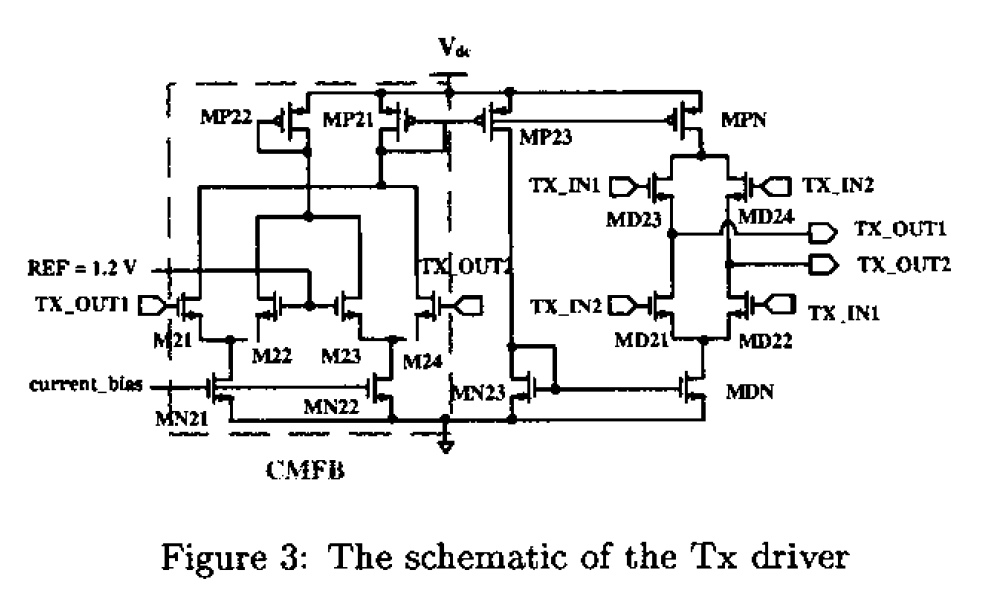
Hi! I design LVDS transmitter. Power supply is 2.5, transistors with thick oxide. Layout is standart: 2 nmos switch, 2 pmos switch, bandgap, bandgap based current reference and CMFB.

In DC this work good: Vos stable. Vol Voh also.

But when modeling transient process there are distortion at the moment of switching. Vos, Voh, Vol go up or down about 50-100 mV.

At the gates of the current source and sink there are also distortions about 20-30 mV.

Source and sink in the saturation region (Vds ~ 1 V). Swithes are in triode region (Vds ~ 70 mV for pmos and ~30 mV for nmos)

What can it be? Are it a bad CMFB, bad matching of transistors, parasitic capacitance or something else?

Tell please about base principle of LVDS driver design.

One more question. What is LVDS predriver? Now i use level shifter (from 1.8 to 2.5) and 2 chain of invertors to equalize V+ and V-. It is predriver? Or predriver is a something else?
 

It might be caused by the loads, especially the capacitance loads.
 

Is the input to your driver full-scale 0-2.5V?
 

Your current source/sink might be going out of saturation. I usually have a pre-driver with a smaller differential voltage driving the final driver.
 

Your current source/sink might be going out of saturation
They can't. Vds ~ 1 V for both.
But probably they can go in weak inversion. There are some distortions (at moments of switching) of they Vg when I modeling transient response.
This distortions about 20-60 mV. But I didn't understand yet why this happens. Vos oscilate -> Vos is input of CMFB amplifier -> So there are oscilations at the output of amplifier -> Output of amplifier is a Vg of NMOS current sink.
But what I don't understand: how distortions of NMOS(current sink) Vg cause distortion of PMOS (current source) Vg?

I checked CMFB loop today. It's stable: Gain at Vos node >50 dB, phase margin > 60 deg.

Can you tell me typical W/L ratios of LVDS driver? I use topology described in paper Gunjan Mandal , Pradip Mandal "LOW POWER LVDS TRANSMITTER WITH LOW COMMON MODE VARIATION FOR 1 GB/S-PER PIN OPERATION" (paper in attachment) but change 4 NMOS switches to 2 NMOS and 2 PMOS.
Now I have:
PMOS current source: 4000/0.4
PMOS switches: 900/0.4
NMOS switches: 600/0.4
NMOS current source: 1000/0.4

Does it seems to be true?
(minimum L = 360nm, for layout I will turn L ~ (600-800) nm, now I want only to uderstand how to tune it).

I usually have a pre-driver with a smaller differential voltage driving the final driver.
Can you advise me papers or books where described this technique?
And tell some basically principles of this technique?

One more question: Vos must be ~ 1.2 when CMFB loop open? Or it's normal that Vos ~ (100-200) mV when loop open?
 

    V

    Points: 2
    Helpful Answer Positive Rating
Your W/L ratios seem a little too big. In my case (up to 1.8GHz), I use 60/0.5 for PMOS and 40/0.5 for NMOS. The current sources are 480/1.2 for PMOS and 412/1.2 but, of course, it depends on the process you are using.
Can you advise me papers or books where described this technique?
And tell some basically principles of this technique?
I don't know of any papers. What I do is very simple: I use an inverter that does not hit the rails so that the top and bottom current source/sink do not go out of saturation.
 

Your W/L ratios seem a little too big. In my case (up to 1.8GHz), I use 60/0.5 for PMOS and 40/0.5 for NMOS. The current sources are 480/1.2 for PMOS and 412/1.2 but, of course, it depends on the process you are using.
Thanks. I would decrease W/L to something like this.
By the way for what process you give W/L?

Sorry, but I don't understand what this mean:
inverter that does not hit the rails
Can you explain?

P,S. Vds of switches should be low? Now I tuned it to ~(80-90) mV for PMOS and ~(20-30) mV for NMOS. Is it correcy? What are principles of Vds of switches tuning? Should it be match or not?
 

But when modeling transient process there are distortion at the moment of switching. Vos, Voh, Vol go up or down about 50-100 mV

If I understand this correctly, both inputs and the vcm (of course) are wiggling. Doesn't that mean that you have CMFB issue?. Does that happen at any frequency? Could it be a too slow CMFB? what is its BW?
 

If I understand this correctly, both inputs and the vcm (of course) are wiggling
I will post picture tomorrow.

Doesn't that mean that you have CMFB issue?. Does that happen at any frequency? Could it be a too slow CMFB? what is its BW?
Hm... I thought that CMFB should correct Vos only over the PVT variations, i.e. CMFB frequency should be low and loop should be stable (phase margin > 60 deg) and have large gain. It is not correct?

I don't remember BW of my CMFB (I will check it tomorrow). What BW should have CMFB usually?
 

Hm... I thought that CMFB should correct Vos only over the PVT variations, i.e. CMFB frequency should be low and loop should be stable (phase margin > 60 deg) and have large gain. It is not correct?
OK, this is the problem! The CMFB BW should be very large, it has to correct for common-mode variation changes at speed and of course, it will work over PVT.
 

OK, this is the problem! The CMFB BW should be very large, it has to correct for common-mode variation changes at speed and of course, it will work over PVT.
Ok. I will verify it tomorrow. But can you tell me what bandwidth I should targer for? And I'm not sure that it is correct (that BW should be large).
I don't understand - I have read in paper (I attached it above) this:
In the amplifier, the first stage's output impedance is high, which in combination with the Miller capacitor creates a low frequency pole. Thus low frequency pole decides the bandwidth of the feedback amplifier. Therefore, without any compensationin feedback network, this low bandwidth diffamp. provides good phase margin even for a wide range of Load (from 0 to 10pf).
Authors said that CMFB amplifier is low BW. Or I didn't understand it correct?
They used large Cm to compensate CMFB amp. How can it be high bandwidth?

And I have read another paper (Andrea Boni, LVDS I/O Interface for Gb/s-per-Pin Operation in 0.35um CMOS). In this paper Boni also used a large cap to compensate CMFB amp. It is imposible that this amplifier have large BW.

However, can somebody answer this questuions:
Vds of switches should be low? Now I tuned it to ~(80-90) mV for PMOS and ~(20-30) mV for NMOS. Is it correct? What are principles of Vds of switches tuning? Should it be match or not?

What is inverter that does not hit the rails?

P.S. JoannesPaulus, tell me please for what process you gave W/L examples.
 

I need to read the paper to answer about the BW question...

The switch is on/off so its vds does not matter, it just has to be big enough to carry the current.
 

JoannesPaulus,
The switch is on/off so its vds does not matter, it just has to be big enough to carry the current.
Thanks. But switch should be in triode region?

Could you tell me techology node for that you gave examples of W/L? Process I used is 180 nm with thick oxide and power supply is 2.5. Should W/L be something like yours?
 

But switch should be in triode region?
It does not matter!

Could you tell me techology node for that you gave examples of W/L? Process I used is 180 nm with thick oxide and power supply is 2.5. Should W/L be something like yours?
Pretty much the same.

One paper I have based my TX I attached above.

I never saw that cmfb implementation before but I would think that the bw of the amp still needs to be large.
 

JoannesPaulus,
I never saw that cmfb implementation before but I would think that the bw of the amp still needs to be large.
Ok. Can you advise me papers where used another CMFB implementation?
 

Here you have a picture of a nice CMFB circuit. It is taken from the paper:

1.0 GBPS LVDS TRANSCEIVER DESIGN FOR LCD PANELS by Chua-Chin Wand , Jian-Ming Huang, and Jih-Fon Huan


There is also a paper by J.E DUQUE-CARRILLO called:

Control of the Common-Mode Component in CMOS Continuous-Time Fully Differential Signal Processing

It makes a fantastic comparison of different CM control circuits
 

Status
Not open for further replies.

Similar threads

Part and Inventory Search

Welcome to EDABoard.com

Sponsor

Back
Top