girih192002
Full Member level 2

- Joined
- Aug 4, 2007
- Messages
- 130
- Helped
- 19
- Reputation
- 38
- Reaction score
- 11
- Trophy points
- 1,298
- Location
- India
- Activity points
- 2,116
Hi,
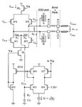
I am working on LVDS Transmitter design and following boni's paper. I didnt understand what would be Bandwidth and gain of CMFB amplifier in this paper and Loop gain and margin.
He has used Compensation Cap = 9.5 pF and Nulling resistor = 1.5 Kohm.
please let me know your suggestions.
I am working on LVDS Transmitter design and following boni's paper. I didnt understand what would be Bandwidth and gain of CMFB amplifier in this paper and Loop gain and margin.
He has used Compensation Cap = 9.5 pF and Nulling resistor = 1.5 Kohm.
please let me know your suggestions.