Majid Rafei
Junior Member level 2

Dear all.
Hi.
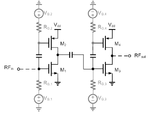
I have a two stage complementary amplifier circuit constructed by CMOS 90nm. Three figures are attached. The first one is the schematic of the amplifier, and the second one is the location of the poles and zeroes of the circuit in an s-plane.
Fig. 1: Schematic

Fig. 2: s-plane

Fig. 3: Frequency Response

As can be seen from s-plane, five poles and two zeros are located below 100 MHz, which two poles and two zeros of them are very close to each other (I think they cancel the effects of each other and the main effects are belong to the three other poles located above them), and also one single pole in about 3 GHz and a couple pole-zero in 6 GHz.
1- According to the third figure, i.e. frequency response, the question is that, what is the main reason of existing a peak in frequencies near 300 MHz. Is that because of the three poles located just below 100 MHz? I think the gain role off above 300 MHz is because of: "the number of poles below 300 MHz is greater than of that above 300 MHz". Am I true?
2- What does make the three poles just below 100 MHz to be created?
Thanks in advance, it will be appreciated for any idea from you.
Hi.
I have a two stage complementary amplifier circuit constructed by CMOS 90nm. Three figures are attached. The first one is the schematic of the amplifier, and the second one is the location of the poles and zeroes of the circuit in an s-plane.
Fig. 1: Schematic

Fig. 2: s-plane

Fig. 3: Frequency Response

As can be seen from s-plane, five poles and two zeros are located below 100 MHz, which two poles and two zeros of them are very close to each other (I think they cancel the effects of each other and the main effects are belong to the three other poles located above them), and also one single pole in about 3 GHz and a couple pole-zero in 6 GHz.
1- According to the third figure, i.e. frequency response, the question is that, what is the main reason of existing a peak in frequencies near 300 MHz. Is that because of the three poles located just below 100 MHz? I think the gain role off above 300 MHz is because of: "the number of poles below 300 MHz is greater than of that above 300 MHz". Am I true?
2- What does make the three poles just below 100 MHz to be created?
Thanks in advance, it will be appreciated for any idea from you.
