Continue to Site
Follow along with the video below to see how to install our site as a web app on your home screen.
Note: This feature may not be available in some browsers.
Ask him for a copy of the syllabus?
If it's an undergraduate class, then the subject matter would be parts like standard logic gates (AND, OR, NOT, NOR, NAND, XOR, etc.), logic devices like multiplexers, counters, and adders. Once you start putting those basic parts together, you can make logic circuits to create decision-based outputs (read from sensors, if some thresholds are met, set some output logic lines, etc).
 , hence i have tried to give you a brief of all concepts while trying to be as clear as possible.. Please prompt me if you didn't understand any point.
Hi again
In some of the posts above I was told that the part "Switching Theory" refers to the fact MOS used as a switching device which turns on/off by sensing the input voltage or whatever. MOS stands for 'Metal Oxide Semiconductor". Is this "MOS" a transistor, diode, or what? I think it's a transistor because a transistor can be used as a switch. What is so special about the "Metal Oxide" prefix? Do we use only those semiconductors to switch on/off the circuits which have been made from metal oxide? Please help me with it. Thank you.
Regards
PG
MOS tells you how the layers of the transistor are put together... metal - oxide - semiconductor. Standard BJT transistors (2N2222, 2N2907, etc) are built entirely using doped silicon semiconductors (N-type silicon, P-type silicon, N-type silicon... thus the name NPN, or PNP for the inverse). A MOSFET device (which is a transistor, because it's a FET = Field Effect Transistor) uses a semiconductor for the drain and source nodes, but a metal gate node. The gate metal is separated from the semiconductor by a highly-resistive oxide layer. This is why MOSFETs don't have any gate current requirements (on the order of microamps due to finite leakage through the package materials).
Other metal-semiconductor devices are available, particularly the Schottky barrier diode. This, however, is just a metal-semiconductor sandwich, no oxide between them (so it's not MOS, but a similar concept in terms of the semiconductor physics that make it work).
Thank you, enjunear.
I couldn't exactly understand the underlined phrase. Would you please help me? What are these "package materials"? The ones which are used to glue the main parts together. Thanks.
Regards
PG

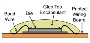
A packaged FET is simply a plastic body, or metal can that hold the semiconductor die and external leads/feet in place. These leads are connected to the die by small bond wires, typically gold and 0.7 to 1.3 mil in diameter. These bond wires arch up inside the package, and then connect to the die. Because you have several (at least 3) wire loops inside the package, you can get coupling between them, just like small antennas in air. Beside coupling through electric field propagation (i.e. antennas) inside the package, the material used to to pot, or fill, the device has a finite resistance, so a voltage difference between two bond wires will result in a small amount of current to flow through the highly resistive encapsulating material.
These signal conduction paths will keep you from obtaining an infinite isolation between pins. Since there is a large resistance from the gate to source nodes on a MOSFET, the current that flows between them is very small, but can typically be measured on the order of microamps. The gist of the story is that you will never have 0 conduction between two dissimilar points, but you can minimize the conduction such that it is very, very small, relative to the signals you are measuring/controlling.
Below are some pictures of how die and bond wires are used inside packaged components.
**broken link removed**
Thanks a lot, enjunear. It was a helpful reply.
So, in your view there are two primary reasons. I don't quite agree with the "antennas" reason because constant DC is used to power the device. For antennas to work we would need constantly alternating current. Where am I going wrong? Please help me with it. Yes, I do agree on the second reason of the material used to pot the semiconductor.
Thank you.
Best regards
PG