Continue to Site

Welcome to EDAboard.com

Welcome to our site! EDAboard.com is an international Electronics Discussion Forum focused on EDA software, circuits, schematics, books, theory, papers, asic, pld, 8051, DSP, Network, RF, Analog Design, PCB, Service Manuals... and a whole lot more! To participate you need to register. Registration is free. Click here to register now.

load pull of EF class amplifier

Inna89

Newbie level 4
Joined
Jul 28, 2023
Messages
6
Helped
0
Reputation
0
Reaction score
0
Trophy points
1
Activity points
70
Hello!
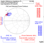
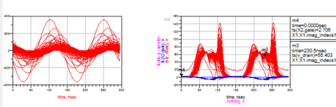
I'm doing research in wireless power transfer (WPT). So I need to do load pull analysis for laboratory amplifier EF class in order to find optimal output impedance of it. Because I'm new in it I have a question: how I should choose impedance of source, input power level and Vbias in order to get quality results?
1691148975774.png
 
This forum has several discussions about optimizing wireless power setups. An Edaboard or internet search can help you as much as anything else.

In comparison there's the old-fashioned 'crystal' radio receiver that needs no power supply. It runs on power from the airwaves (radio waves). It's built around a coil and capacitor. Usually one or the other is tunable.

I think the main optimizing is in making your receiver's resonant frequency match the sending frequency.

You want the resonating circuit to produce sufficient voltage so that it overcomes diode thresholds and/or battery voltages. You want it to produce sufficient current to be of practical use.
This can be done by certain size of receiving coil, and suitable combination of values of coil and capacitor. The values should allow sufficient Ampere level at your sending frequency.

As it turns out there's a certain combination of voltage and current going through your circuit that accomplishes the above. After you read about other experimenters' results it becomes clear that you're lucky if you can generate enough power to light a plain red led.
 
THa
This forum has several discussions about optimizing wireless power setups. An Edaboard or internet search can help you as much as anything else.

In comparison there's the old-fashioned 'crystal' radio receiver that needs no power supply. It runs on power from the airwaves (radio waves). It's built around a coil and capacitor. Usually one or the other is tunable.

I think the main optimizing is in making your receiver's resonant frequency match the sending frequency.

You want the resonating circuit to produce sufficient voltage so that it overcomes diode thresholds and/or battery voltages. You want it to produce sufficient current to be of practical use.
This can be done by certain size of receiving coil, and suitable combination of values of coil and capacitor. The values should allow sufficient Ampere level at your sending frequency.

As it turns out there's a certain combination of voltage and current going through your circuit that accomplishes the above. After you read about other experimenters' results it becomes clear that you're lucky if you can generate enough power to light a plain red led.
Thanks for your answer. I done optimization for coils geometry in order to met the system requirements of voltage to current ration, delivered power and efficiency. And I see at resonance condition at the primary side (at transmitter resonant circuit) input impedance is about 10 Ohm. This is non-optimal impedance for power generator. So the system efficiency is smaller than can be. In order to achieve the maximum of system efficiency I need to modify output Pi-network of power amplifier and I want to do it through load-pull analysis technics. I tried to do load-pull analysis (one tone) with different values of Vbias and source power and the results was different. So, my question is about how to set correctly Vbias, source impedance and power level for load pull analysis of EF class amplifier?
 
Hi,

In ADS you have templates for Load Pull simulations, available in a schematic: Design guide-> Load Pull. Select the analysis you prefer and insert your transistor, the Vbias and input powers.
1691760280083.png

This template has all neccessary plots to check what is the optimal output impedance for your transistor.
1691760433757.png

Check out ADS Load Pull DesignGuide for more help
Then, you have to design your output matching network to go from Zoptimal to Zo (usually 50 Ohms).

Regards
 
Hi,

In ADS you have templates for Load Pull simulations, available in a schematic: Design guide-> Load Pull. Select the analysis you prefer and insert your transistor, the Vbias and input powers.
View attachment 184341
This template has all neccessary plots to check what is the optimal output impedance for your transistor.
View attachment 184342
Check out ADS Load Pull DesignGuide for more help
Then, you have to design your output matching network to go from Zoptimal to Zo (usually 50 Ohms).

Regards
Hi! Thanks for your answer. I've done load pull analysis with template as you said with schematic of generator and value of bias voltages Vbias_1=4V, Vbias_2=30V; power source level Pavs_dBm=25 and impedance of source Z_source_fund = 5+j*0.

1692006110893.png


After successful simulation I got this results:
1692006323073.png

Also, I plotted time diagrams of drain and gate voltage and drain current , Power (in W) and PAE rectangle plots:
1692006813326.png

But as I see this results are not correct because the drain voltage waveform not correspond to reference EF2 class waveforms (yellow and blue) from GSWP300W manual:
1692007399579.png

Also levels of load Power and PAE are not valid, because reference values of this parameters are:
1692007669162.png

At VDD=30 V the output power must be 26 W and PAE about 90%.
The main problem as I see isn't correct sets for Vbias_1, Vbias_2, Z_source and source power. I tried to analyze with different combination of this parameters, but the results were more worst. So, my questions are:
1) which method I should use for correct choice of this parameters?
2) what type of gate voltage waveform I should see at One Tone Load Pull simulation of switching amplifiers (sinusoid or rectangle)?
3) Can Two Tone Load Pull simulation help me to get desirable waveforms?
 
Hi! Thanks for your answer. I've done load pull analysis with template as you said with schematic of generator and value of bias voltages Vbias_1=4V, Vbias_2=30V; power source level Pavs_dBm=25 and impedance of source Z_source_fund = 5+j*0.

View attachment 184402

After successful simulation I got this results:
View attachment 184403
What I see here is that you have change the values of Sload to sample different values of load because your load pull doesn't show all its values.

Your have to sample another points: change values S_imag_min, S_imag_max, S_real_mi and S_real_max and you will see that the rectangle of black dots on your smith chart change location and size. You have to locate it where you can see maximum points of PAE and Pout.


Also, I plotted time diagrams of drain and gate voltage and drain current , Power (in W) and PAE rectangle plots:
View attachment 184406
But as I see this results are not correct because the drain voltage waveform not correspond to reference EF2 class waveforms (yellow and blue) from GSWP300W manual:
View attachment 184408
Also levels of load Power and PAE are not valid, because reference values of this parameters are:
View attachment 184409
At VDD=30 V the output power must be 26 W and PAE about 90%.
The main problem as I see isn't correct sets for Vbias_1, Vbias_2, Z_source and source power. I tried to analyze with different combination of this parameters, but the results were more worst. So, my questions are:
1) which method I should use for correct choice of this parameters?
2) what type of gate voltage waveform I should see at One Tone Load Pull simulation of switching amplifiers (sinusoid or rectangle)?
3) Can Two Tone Load Pull simulation help me to get desirable waveforms?

If think maybe your problem is realated with that I have mentioned before. Let me know if you find more problems.


regards
 
What I see here is that you have change the values of Sload to sample different values of load because your load pull doesn't show all its values.

Your have to sample another points: change values S_imag_min, S_imag_max, S_real_mi and S_real_max and you will see that the rectangle of black dots on your smith chart change location and size. You have to locate it where you can see maximum points of PAE and Pout.


If think maybe your problem is realated with that I have mentioned before. Let me know if you find more problems.


regards

Thank you for your answer!
I've done simulation with another points of Sload (S_imag_min=-0.2; S_imag_max=0.9; S_real_min =-0.9; S_real_max=-0.1)
and get this results:
with Vbias1=1V; Vbias2=30 V; Pavs=45dBm; Z_Source_Fund=0.005+j*0
1696697334767.png
1696697497996.png


This results are differs from datasheets (26W, 90%, 50 Ом), so I did simulation with other value of Z_Source_Fund = 0.01+j*0. I get this results:
1696697819010.png
1696697893263.png

This result is better but the value of PAE, Zload_opt, Power are still differs from datasheet.
I also did simulation with another values of Vbias1=0V; Pavs=45dBm with Z_Source_Fund=0.005+j*0:
1696698287714-png.185338
1696698369200.png

I get 90% PAE, but Power level is big, time domain signals are distortion and Zload at the max PAE is very far from optimal 50 Ohm.
I simulated real amplifier with output matched networks. I tested this amplifier in laboratory with Rload=50Ohm and get 90% PAE with time domain signal very similar with datasheet's.
So, I don't know what I should be do to get similar results in ADS. As I see Z_Source_Fund, Vbias1 and Pavs must be chosen carefully, but I don't know how do it...
Have you any idea?
Regards
 

Attachments

  • 1696698287714.png
    1696698287714.png
    139.9 KB · Views: 88
  • 1696698314429.png
    1696698314429.png
    43.8 KB · Views: 38
Hi!

What datasheet are you using? I can't find the one with load pull measurements.

You can use a Z_Source_Fund similar to datasheet's one. Z_Source_Fund=0.005+j*0 looks very low.
What time domain signal are you using?

By the way, what application will have this amplifier?

regards
 
Hi!

What datasheet are you using? I can't find the one with load pull measurements.

You can use a Z_Source_Fund similar to datasheet's one. Z_Source_Fund=0.005+j*0 looks very low.
What time domain signal are you using?

By the way, what application will have this amplifier?

regards
Hi!
I use "GSWP300W-EVBPA-Technical-Manual-Rev-220215-1.pdf" (p. 19,26) to compare Vds time domain signal, efficiency and power level. Also, I use "Class-EF2-PCIM_2018_Manuscript.pdf" which contain information of load pull analysis quite similar GaN amplifier.
This amplifier is switching type and used as power source of transmitting resonant coil in Wireless Power Transfer applications. It is controlled by 5V Vgs rectangle pulses with 70% duty cycle.
In the load pull analysis I use sinusoid power source, Vbias1, Z_Source_Fund and try to set the same operation point of transistor.
Regards
 

Attachments

  • GSWP300W-EVBPA-Technical-Manual-Rev-220215-1.pdf
    2.1 MB · Views: 43
  • Class-EF2-PCIM_2018_Manuscript.pdf
    988.6 KB · Views: 44
Last edited:
Hi!
I use "GSWP300W-EVBPA-Technical-Manual-Rev-220215-1.pdf" (p. 19,26) to compare Vds time domain signal, efficiency and power level. Also, I use "Class-EF2-PCIM_2018_Manuscript.pdf" which contain information of load pull analysis quite similar GaN amplifier.
This amplifier is switching type and used as power source of transmitting resonant coil in Wireless Power Transfer applications. It is controlled by 5V Vgs rectangle pulses with 70% duty cycle.
In the load pull analysis I use sinusoid power source, Vbias1, Z_Source_Fund and try to set the same operation point of transistor.
Regards
Hi!

I saw that in the application they are using a push-pull configuration of this transistor (2 GaN transistors). Is your Load Pull for one or two transistors? you have to take into account this because it will change the output form. This configurations also helps with distorsion issues, reducing harmonics.


1697023271638.png

1697023299909.png


Keep in mind that load is the paper is sometimes 30Ohms instead 50, that will change maximum power. (Power = I*R^2)

It is also important the Vdrain that you chose, it will affect your efficiency and power.

Very interesting application, thank you for the information

Regards
 
Hi!

I saw that in the application they are using a push-pull configuration of this transistor (2 GaN transistors). Is your Load Pull for one or two transistors? you have to take into account this because it will change the output form. This configurations also helps with distorsion issues, reducing harmonics.


View attachment 185393
View attachment 185394

Keep in mind that load is the paper is sometimes 30Ohms instead 50, that will change maximum power. (Power = I*R^2)

It is also important the Vdrain that you chose, it will affect your efficiency and power.

Very interesting application, thank you for the information
Hi!
Thank you for answer. I'll do simulation within your recommendations.
Regards
 

LaTeX Commands Quick-Menu:

Similar threads

Part and Inventory Search

Welcome to EDABoard.com

Sponsor

Back
Top