GSarris
Member level 1
- Joined
- Mar 27, 2009
- Messages
- 41
- Helped
- 0
- Reputation
- 0
- Reaction score
- 0
- Trophy points
- 1,286
- Location
- Netherlands
- Activity points
- 1,616
LNA simulation results
Hello,
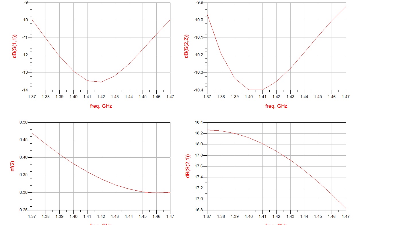
I designed an LNA at 1.42GHz based on the NE3210s01. My BW is 100MHz and i get the following results. Nf=0.47dB, S11=-36 at my center freq and -13db worst over the band, a gain of 17dB approximately constant over the band and S22=-6dB at my center freq and -4dB worst. I wonder if my S22 is acceptable. My LNA is destined to be the first stage of a radio telescope. please provide me with your opinion.
Thanks in advance,
George
Hello,
I designed an LNA at 1.42GHz based on the NE3210s01. My BW is 100MHz and i get the following results. Nf=0.47dB, S11=-36 at my center freq and -13db worst over the band, a gain of 17dB approximately constant over the band and S22=-6dB at my center freq and -4dB worst. I wonder if my S22 is acceptable. My LNA is destined to be the first stage of a radio telescope. please provide me with your opinion.
Thanks in advance,
George