Continue to Site

Welcome to EDAboard.com

Welcome to our site! EDAboard.com is an international Electronics Discussion Forum focused on EDA software, circuits, schematics, books, theory, papers, asic, pld, 8051, DSP, Network, RF, Analog Design, PCB, Service Manuals... and a whole lot more! To participate you need to register. Registration is free. Click here to register now.

LNA TRF37D73 unexpected distortions

Bobson2000

Junior Member level 2
Joined
Aug 23, 2023
Messages
20
Helped
0
Reputation
0
Reaction score
0
Trophy points
1
Activity points
292
Hi.

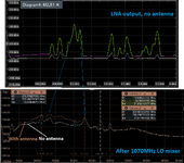
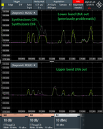
Im launching radio receiver for two bands. First RF path is common and containst two LNAs, next the path is splitted to two channels. Each channel starts with pass-band filter, and LNA TRF37D73 after him. First channel/band with center freq 1575MHz works well, i have about 8mVpp on LNA (U21) out , when antenna input is floating/matched. But on second channel/band with center frequency 1232MHz have some problem - on LNA (U18) output i get floor about 20mVpp, with unexpected jumps to 25, 30, 40mVpp (one time i got about 240mVpp). Jumps are unexpectable time, form couple microseconds, to couple of miliseconds. This signal level causes ADC overload on end of path. With eliminating method i come to conclusion that problem source is U18 LNA.
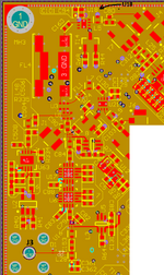
On LNA's outputs circut was the same schematics - has just matching bias coil - series capacitor - UFL connector when im measuring. PCB layout is in some part different. TRF37D73 is unconditionable stable LNA.

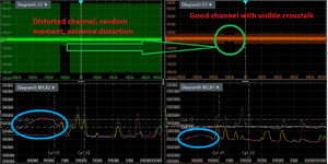
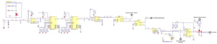
1. Probably most significant test i have don was: crossing channels on LNAs (U18,U21) inputs (on C160,C130) - distortion still occurs in the same channel which contain U18 - so i think everything before LNA's can be eliminated from suspects, including pasband filters. Second channel looks proper, have just some crosstalk form distorted channel
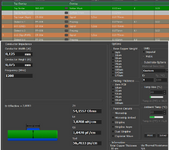
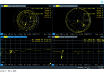
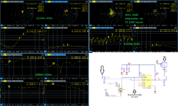
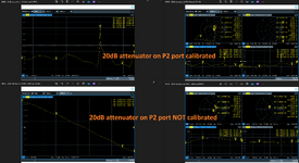
2. I measured LNA in PCB, by VNA for full VNA band 100k-6GHz. Gain looks property, S11 max value is about -3dB (so it should be stable), in interesting band is about -18dB. S11, S22 impedances
looks proper, S22 is distorted but i used 20dB attenuator on P2 port.
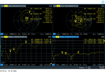
3. I measured stage with splitters and pasband filters by VNA, and for my band it looks proper (S11, S22 impedance). Filter has own in/out impedance matching. I do not measured it on full VNA frequency range, but i will do it further.
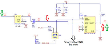
4. I tried too: changing LNA supply source, adding 10u, 1u, 100n capacitors to LNA supply, connecting supply direct from C101 to LNA on top layer (is not done on PCB layout as You can see), connecting supply by ferrite bead, adding resistor (10R) in series to biasing output coil, with 10p and 100n capacitors, changing this coil to producer suggestes 100nH, adding ~800R resistor shunt on LNA input, replacing LNA, filter, connecting directly LNA input to filter input, or splitter input/output (of course removing filter/splitter), "adding" vias to supply capacitors (by connecting it with vias stitching). I tried to place finger on supply decoupling capacitors, and distotrion not decerases, but incerases about 30%.
5. I readed some topics about LNA oscillating issues, and stability, i tried some suggested there solutions, but no find no working solution in my case, and now im near hit the wall :). I tried all this solutions/changes, but i don't see significant or "going to better way" solutions.
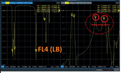
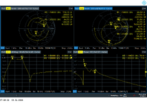
6. Now im trying to get possible impedance mismatch caused by SAW pass-band filter on out band frequencies, because when i just short LNA input by 50R i get proper value on LNA out (in progress). Filter in first channel/band has external matching coil (as datasheet suggest), but in distorted channel/band i will probable need them too.

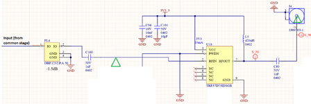
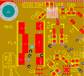
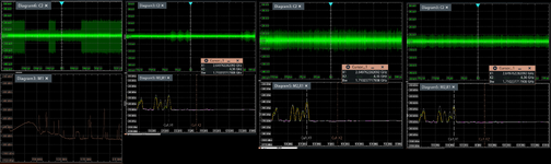
I added some graphics: piece of layout, schematic, and measured by VNA: LNA, splitter to filter stage (J1-FL4), measured distortions on LNA out. Did You have some sugestions, what should i try, or meas?
Best regards.
 

Attachments

  • U18 sch.png
    U18 sch.png
    180.1 KB · Views: 75
  • U18 input - J4 output, 0,1-6GHz, cal 20dB att on P2 (soldered SMA cable) (1).PNG
    U18 input - J4 output, 0,1-6GHz, cal 20dB att on P2 (soldered SMA cable) (1).PNG
    78.2 KB · Views: 77
  • J1-FL4 out, without C160 (measured by soldered SMA cable)(2).PNG
    J1-FL4 out, without C160 (measured by soldered SMA cable)(2).PNG
    76.2 KB · Views: 62
  • U18 pcb.png
    U18 pcb.png
    429.3 KB · Views: 87
  • U18 LNA out distortions.png
    U18 LNA out distortions.png
    2.1 MB · Views: 83
Last edited:
I wonder about PCB stack-up. Either substrate unusual thin so that the traces are halfways matched to 50 ohm, then components pads create big parasitic capacitance or traces are much too thin.
 
Thanks for quick answer. Here i add piece of stackup, and impedance check for RF paths on TOP layer. It's look OK. Path has width 0,125mm. Unusal thin - You mean first (Dielectic1) prepreg thickness too thin? And example FL4 (filter) big pads are acting as real capacitors?

I measured S parameters from first splitter input, to FL4 pass-band filter output for 100k-6GHz band, and results i give below. I think for pass-band it looks not much very well (ex M2 in S22), but not that bad to cause this scale disturbances (i think). My worries are raised when i look at S parameters for out of band, for example S11 on start frequency is about -0,3dB. I compared this with MiniCircuts SMA original pass-band filter and it has <-15dB S11, S22 in pass-band, and out of band max value is about -0,5dB in S22. I should do the impedance matching for this filter? I think about high-pass impedance matching circut.
 

Attachments

  • Stackup and Top impedance.png
    Stackup and Top impedance.png
    262.3 KB · Views: 59
  • J1-FL4 out (soldered SMA cable) 100k-6G.PNG
    J1-FL4 out (soldered SMA cable) 100k-6G.PNG
    74 KB · Views: 50
The datasheet of DBP.1232.P.A.50 shows that the return loss of the filter is better than -15dB without any matching components. So, there you may have a layout problem.
You mentioned that you checked for stability. You did this using the scope or the Spectrum Analyzer? An SA gives better information about potential oscillations.
Adding a series resistor (25 to 100ohms) in series with the L5 may avoid oscillations, at the expense of bit lower OIP3.

Meanwhile, 3.25dB noise figure for an LNA is a lot nowadays. If you add the 1.5dB insertion loss of the filter you arrive to a 4.75dB noise figure for the entire front-end, which doesn't make sense when there are better LNAs on the market:


vfone
Thanks for information about noise figure. About -15dB return loss of this filter - my measurement (S22) doesn't look that bad in reference to datasheet. You thinkg bout layout near this filter - yes? I use VNA, but i have oscillosopce with FFT function, as You see on last graphics in first post. For fast test i addes about 50Ohm resistor before L5 and i see no significant change. Tommorow i will try grater values and adding capacitor 10p and 10n as on TRF37D73 evalboard.

On the graphics below i show extremal distortions (today it doesn't occurs), and what is strange/interesting: distortions marked in blue ellipses occurs sometimes, they rise, and fall in random time, but other peaks (to right on FFT) are still present with small level changes/bumping.
 

Attachments

  • Two channel distortions.png
    Two channel distortions.png
    107.5 KB · Views: 52
It oscillates at Output Side.( S22 is not normal ).
A typical RF layout should look like
1704817403586.png
 
Last edited:
FvM
Yes, some peaks are from telephony, I have BTS in the area and Wi-Fi is also visible, but I still don't know why it gained too much.

BigBoss
S22 may be misleading as I have a 20 dB attenuator on the P2 VNA port and as I see it, adding an attenuator (included in the calibration) maximizes S22 "diffuse". But I will try to add an attenuator on the P1 port and connect P2 directly to the VNA, because the solution, as you mentioned, is most likely related to the amplifier output.

Currently, I have eliminated the ADC overdrive by powering L5 through a resistor of up to 330R (!) and I have achieved the correct signal level - attenuated about 20dB. But I still don't know how to solve the problem in the next PCB revision, so I will look for solutions. So You think the layout is the main source of problem?
U21 (the second twin track) has a similar layout, visible in the photo from the first post, and it is OK there, so I think what I can mainly change?
 
Layout is a part of problem. You should also use screening to eliminate external contributors such as GSM, WIFI etc.
But the schematic is not complete. Potential oscillation might come form different sources. If you post your whole schematic here, I can lead you better.
Transmission Lines seem to me not correct. they have to have 5.06mils track width. But his is very narrow due to di-electric height.
 
BigBoss
1. You mean screening as coplanar wave, or EMC cage? PCB will be mounted in metal enclosure of course.
2. Transmision line microstrip is 4,9mil, when distance to reference plane is 2,95mil - i readed that exist rule that says the line width should be 2x distance to reference plane, taking into account the impedance calculations of course. Diamensions was made with about 15% accuracy (PCB manufacturer) - You think it have sense to do the coplanar wave with this PCB manufacturing accuracy? It has sense for this frequency systems?
3. In next revision i planed to:
- replace filter with much smaller packagege
- connect floating LNA pins to GND (which i kind of expect)
- add series resistor, and decoupling capacitors for L5 bias coil
- connect LNA supply just on top layer, and use proper capacitor values
- use coplanar wave - has it sense?
- in sum - copying EVM (evlboard) circut :)
4. Schematic. From antenna input i have: LNA BGA824N -> 2x switched attenuator -> LNA BGA824N - two splitters NP2G+ (split to two bands paths) -> band-pass filter (FL4) -> problematic LNA (U18) -> impedance match balun -> downcounting mixer -> low pass filter -> LNA and ADC, but the signal path is cut on U18 output (goes to UFL), so i think the next components doesn't take a part in out distotrions (proper?). I must ask for permission to publish more schematics.
5. Interestingly, the emerging unwanted signals do not add to the signal from the antenna, but begin to "fade out" in terms of power (graphics below - antenn connected vs unconnected).
 

Attachments

  • LNA out, mixer out comparision.png
    LNA out, mixer out comparision.png
    199.4 KB · Views: 41
Last edited:
There are two essential problems here.
Some carriers ( GSM, PCS, LTE, TV etc.) are intervening to the system so this can be eliminated with a well screening.( Measurements can be done in a EM Chamber)
But there is/are some oscillation(s) that impact the performance of the circuit. Because there is a peak 1.2GHz and there is nothing in the spectrum.
If you can supply schematic and layout I can tell you something concrete, otherwise discussion cannot lead.
 
I get permission. And attached schematic and layout.
 

Attachments

  • Brd - copy.png
    Brd - copy.png
    472.6 KB · Views: 56
  • Sch — copy.png
    Sch — copy.png
    245.7 KB · Views: 55
If you measure the Response of this chain at J4, it's a big mistake. There is a Balun after that and if the Mixer is not connected, it will mislead you much.
I said one in a topic, RF design must be forwarded step by step. You have to be sure there is no oscillation from Output to Input.
The Output stage must be measured first under "Normal" conditions then the measurement should be rewind trough the Input.
Disconnect C80 and disconnect FL4 from previous stage and connect a semi-rigid coaxial cable to its input and measure.
Also, VIAs are very few around critical components especially de-coupling capacitors. I don't know the Transmission Lines are correct (suppose to be)
 
So, the first start of the radio (receive) path should look like this: I first perform measurements on each component (LNA, filter, splitter) separately using VNA (SA too?)? And only when these measurements show that the LNAs are stable and the impedance matching is quite good, can the track be connected into a whole - right? Do you know any literature/tutorial from which I can learn this? I'm a beginner and while structures are sometimes described, his launcing is described less frequently. When first launching the track, there is not always a connector to connect the coaxial cable, and its soldering causes some disturbance in VNA measurements.

The LNA TRF37D73 is listed as "unconditionally stable" in the documentation. I will measure S22 again and I should probably expect the magnitude value to exceed 0. Do you suggest connecting the VNA as in the attached graphic with green arrows? I was thinking about measuring according to the red arrows.

I am aware of the vias, but such a project has already been done and I am just launching it.
 

Attachments

  • U18_vna.png
    U18_vna.png
    186.6 KB · Views: 42
So, the first start of the radio (receive) path should look like this: I first perform measurements on each component (LNA, filter, splitter) separately using VNA (SA too?)? And only when these measurements show that the LNAs are stable and the impedance matching is quite good, can the track be connected into a whole - right? Do you know any literature/tutorial from which I can learn this? I'm a beginner and while structures are sometimes described, his launcing is described less frequently. When first launching the track, there is not always a connector to connect the coaxial cable, and its soldering causes some disturbance in VNA measurements.

The LNA TRF37D73 is listed as "unconditionally stable" in the documentation. I will measure S22 again and I should probably expect the magnitude value to exceed 0. Do you suggest connecting the VNA as in the attached graphic with green arrows? I was thinking about measuring according to the red arrows.

I am aware of the vias, but such a project has already been done and I am just launching it.
Yes, absolutely. Divide the circuit into pieces and do the measurements separately and be sure that all separated blocks work well then connect them again step by step.
You can use semi-rigid coaxial cables with connector mounted while measurements.
There is no literature about these methods, every circuit/system will teach you something. Or you ask to experienced engineers like us. But you cannot find any textbook that explains such things.
TRF37D73 might be "unconditional" stable but these oscillations might come from different blocks, you cannot see that at a glance.
Do your measurement which you have mentioned before and let see what there is.
 
This is partly how I started, but all I saw were some impedance mismatches in a few places, but I was measuring not individual components, but segments, for example 2 LNAs and a filter (what was between the UFLs), what was wrong i mean now.

I measured U18 using VNA. I left C160 and C80 because I was afraid of the impact of a possible DC on the VNA ports, although from what I read, and according to the marking on the VNA ("+27dBm/30VDC"), it can be connected without these capacitors - does it have a significant impact on the measurement results? ? I prefer to ask before I connect without capacitors (I remember that you told me to remove them, but for fear of the equipment I prefer to do it in two steps).

I have added my measurement results below - S11, S22 do not even approach level 0, so I interpret this result as: LNA stable, no oscillations. In such a case, to make sure, I should reach for the SA, short-circuit the LNA input (via 50Ohm) and measure the output - I should see bands at the oscillation frequencies - I think correctly. I have done VNA measurements in two freq ranges: 0,5G-2G, and 100k-6G.

Thank you for helping me :)
 

Attachments

  • VNA direct meas.png
    VNA direct meas.png
    271.6 KB · Views: 50
I see still an oscillation but this oscillation is definitely coming from the Input side.
Question : If there is an Input related oscillation why we don't see this oscillation at the Output of the LNA ??
It might be coming from another source ?? Control MOS transistor ?? There should be another issue.
 
Last edited:
What on the graph indicates that oscillations are occurring? I don't see S22/S11 going above 0 (unstability indicator), just one thing which looks "suspicious" is strong valley in S22 dB Mag chart, but is not on expected frequency, and had nothingh to say in oscillation thread (i think). I see "wavy" S11 too, form start to about 1,3GHz. I should use SA to see its clearly?
I excluded transistor from suspects, because his pin connected to LNA is shorted do GND on PCB by piece of wire to be sure that LNA is constantly enabled, but oscillations occurs when the wire was absent too (voltage on PD pin was about 0,68V so LNA was enabled too).

Good news:
I made a step back, and i remind myself that second band path has the same problem (about 1,2GHz), but signal is attenuated by pasband filter (about 1,5-1,6GHz), so i don't payed attention for this, because it not influence on my usable signal. So unconected supply for two synthesizers (LMX2581 - sources of LO for mixers), and problem dessapear, so the source of this 1,2GHz, (and near) distorting signal are synthesizers. For now, the path of the disruption is unknown, i will try to add some ferrite beads to synhtesizers supply, or try to some another separation methods, and will try to measute it by near field probe, and i will let You know what happend.

Below graphis with comparition two bands paths.
 

Attachments

  • M2-J4, M3-J6, U4 OFF, REF - U4 ON, supply ON — copy.png
    M2-J4, M3-J6, U4 OFF, REF - U4 ON, supply ON — copy.png
    50.9 KB · Views: 35
Well done..
So either the power supply rails are also dirty OR EMI impacts the other blocks OR Both... Therefore you have to re-design this PCB in my humble opinion.
Power Supply Rails, Decoupling, Screening, Symmetry Features, Guiding the Transmission Lines, Isolation all they are extremely important for RF systems.
That's why RF PCB Design needs a special attention and care.

Note : If there is an oscillator either discrete or integrated, this oscillator MUST be absolutely screened to prevent other circuits from disturbtion. My recommendation is to screen this PLL+MIX block ( even a temporary with a piece of tin metal or copper metal pieces.) with GND connections.
OR, power OFF all rest circuit blocks and measure this chain only. (Best option to debug the problem)
 
Thanks Big Boss.

I made several dozen measurements and changes in two PCBs to diagnose the problem, and i don't meet strong distortions on U18 LNA output now, but i can't get this glitch back even by undoing the changes to the PCB, so I'm a bit lost, and i don't know what helped... So, now i removed series resistor to this LNA output bias coil (L5). ADC is not overloaded. I think this problem will be come back, when i will launch next PCB (cause i have couple of not used PCBs), but now im little confused.
I tried to reduce some spurs coming from clock synthesizer with adding beads to first two LNAs, but they still exist, they lost when i get this synthesizer to power down mode, so - thats sglitch source (LMK04906 disturb on several frequencies, LMXs2581 disturb just on mixer LO frequency). I tried screening first, most low-signal stage of RF path, but no effect. So i think in next PCB revision i neet to add some EMI gasket on synthesizers, and some for low-signal stage of RF. GSM, and WiFi, which strongly mislead my perception, don't impact to much, so i need live with it.
I discovered too, that the pass band filter in lower band has slightly saying "not perfect" characteristics (S21) in about WiFi/LTE region.

I have three questions:
1. Now im doing VNA measurement of whole RF path, each significant component singly. I attched photo from one of measurement - tell me is that technique proper? Measurement results looks reliably.
2. It' good idea to do RF paths on PCB from J3, to first LNA as coplanar wave? And via stithing barrier (GND) between clock synthesizers, and rest of PCB, when some of internal layers are power/signal layers? I ask about this two, because i have several another ideas "what to change" in next PCB revision.
3. When im measuring LNA by VNA i need to add attenuator, to not burn VNA. I measured one LNA (TRF37D73) in two ways for test: 20dB attenuator on P2 included in calibration, and no included in calibration, but added after calibration. I added results in attachement. I know that attenuator should be calibrated, because if not, it will become a part of DUT (results to trash?). I readed some document from Agilent about im confused after measurement. I want to add that in one point of chart You can see gain above 2x declared gain, but how to avoid that situations - i have -10dBm power, and 20dB attenuator so it was safe, but it was unexpected. How to do it properly, step by step?
 

Attachments

  • M5 (4) — copy.jpg
    M5 (4) — copy.jpg
    4.1 MB · Views: 35
  • low band - band pass filter FL4.PNG
    low band - band pass filter FL4.PNG
    351.7 KB · Views: 30
  • attenuator calibrated vs uncalibrated.png
    attenuator calibrated vs uncalibrated.png
    914.6 KB · Views: 40
Last edited:

LaTeX Commands Quick-Menu:

Similar threads

Part and Inventory Search

Welcome to EDABoard.com

Sponsor

Back
Top