Continue to Site

Welcome to EDAboard.com

Welcome to our site! EDAboard.com is an international Electronics Discussion Forum focused on EDA software, circuits, schematics, books, theory, papers, asic, pld, 8051, DSP, Network, RF, Analog Design, PCB, Service Manuals... and a whole lot more! To participate you need to register. Registration is free. Click here to register now.

[PIC] LM35CZ > Amplification Chain to DAC

Eric_O

Advanced Member level 4
Joined
May 31, 2020
Messages
104
Helped
0
Reputation
0
Reaction score
0
Trophy points
16
Activity points
996
1) Calculation of the mounting characteristics for a full-scale variation of the ADC :

I chose a measurement range between -10 °C and +100 °C with a 10-bit analog/digital conversion, i.e. from 0 to 1023, i.e. 1024 values. In absolute terms, the temperature range is therefore 10 °C + 100 °C, i.e. 110 °C.

Powered by a voltage of 5 V, the per-bit resolution of the 10-bit analog-to-digital converter (ADC) is 5 V / 1024 different values, or 4.88 mV each time one of the 10 bits changes state, from 0 to 1 or from 1 to 0. 4.88 mV is the resolution in volts per bit. This is the quantum q of the 10-bit converter (1).

On the one hand, we have a sensor output voltage that will vary between 0 and 110 °C x 10 mV, i.e. between 0 and 1100 mV. On the other side, there is a 10-bit analog-to-digital converter (ADC) that will convert a voltage that varies over a range of 0 to 1100 mV into input.

While powered at 5 V, the ADC could convert a voltage that varies from 0 to 5 V as input.

The solution is to amplify the voltage range from 0 to 1100 mV over a voltage range from 0 to 5 V with an op-amp amplification circuit.
  • input voltage Vi = 1100 mV, i.e. 1.1 V,
  • output voltage Vo = 5 V.
Thus amplification A = Vo / Vi = 5 V / 1.1V = 4.545

2) Problems related to the treatment of sub-zero temperatures :

LM35 Temperature Sensor Linear Relationship :

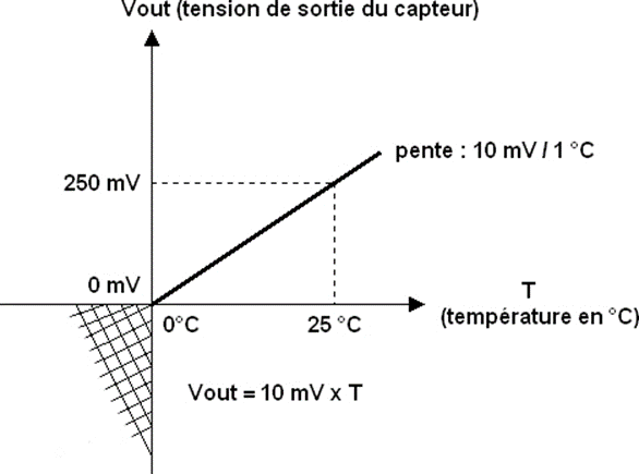
The LM35 sensor has the following linear characteristic V out = f (T) :
1709812448595.png

Managing sub-zero temperatures with an LM35 :

The T = f (V) characteristic of the LM35 temperature sensor has a breakpoint for a temperature of 0 °C. This is due to the intrinsic feature of the sensor, which only measures positive temperatures.

However, if you want to measure a temperature range of -10 °C to 0 °C and from 0 °C to 100 °C, it is necessary to make a reference change on the sensor characteristic above.

In electronics, this change of reference is equivalent to moving the operating point of the LM35 by adding a new DC voltage called offset to the sensor's output voltage (proportional to temperature).

Synoptic:

1709812534614.png


Determination of the offset voltage for measurement from -10 °C to +100 °C :

We need to make sure that we get a potential at the ADC input of 0 volts for a measured temperature of -10 °C. Since ADC cannot measure negative voltage, its conversion range is between 0 volts and 5 volts.

Knowing the scale factor of the sensor (10 mV / °C), we can write :

- 10 °C x sensitivity = -10 °C x 10 mV = -100 mV

Its absolute value is therefore 100 mV.​
Knowing that we have an amplification factor A = 4.545, we can write:

100 mV x A = 0.1 V x A = 0.1 V x 4.545 = 0.4545 V = 454 mV.​

Thus, the offset voltage introducing the offset will be V offset = 454 mV.

This offset voltage allows the operating point (displaced bias) of the LM35 sensor to be shifted, so that it delivers a consistently positive potential for temperatures between -10 °C and 0 °C.

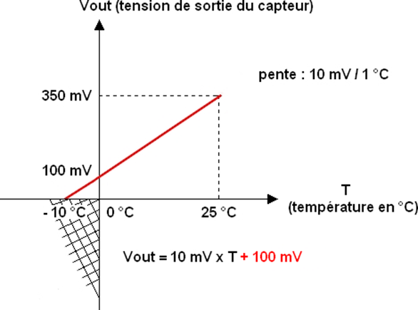
This is equivalent to introducing a change of reference on the sensor characteristic such as:
1709812656406.png


The operating point of the LM35 has been moved so that 100 mV is obtained at an intrinsic temperature of 0 °C.

Thus the linear relation is now written: V out = 10 mV x T + 100 mV.

Nevertheless, this potential is a figment of the imagination because it is in practice not measurable because it is always associated with an offset voltage.

Because of this stratagem (displaced operating point) the "negativity" of the intrinsic voltage of the sensor for T = -10 °C is all relative, because it actually means nothing more than that of the voltage present on pin 2 of the sensor is at a potential 100 mV lower than that existing on pin 3.

Our measuring range will therefore be between -10 °C and +100 °C.

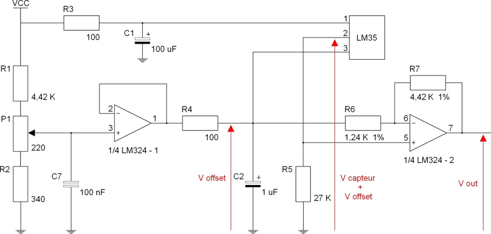
3) Acquisition chain between the LM35 and the microcontroller :

Scheme:
1709812833438.png


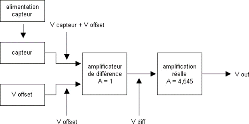
Equivalent diagram of the acquisition chain :
1709812902578.png


Here are the different theoretical potentials of the equivalent scheme. This is a figment of the imagination, because in fact V out and V diff are not measurable in practice. Indeed, the first potential is always associated with V offset and for the second it is an integral part of the "difference amplifier" stage.
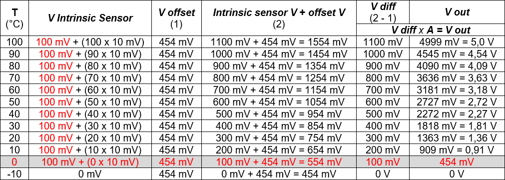
1709813049709.png


The "A" amplification is performed from an operational amplifier mounted as a non-inverting difference amplifier.

A = (1 + R7 / R6)

Let's maintain the value of R6 and calculate the value of R7 for an amplification A = 4.545.

4,545 = (1 + R7 / 1,24 Kohm)

R7 = 4395,8 ohm = 4,39 Kohm

4.39 Kohm is between the standard resistance values of 4.22 K and 4.42 K.

Let's calculate A with the lower standard value and the upper standard value in order to get closer to the value of 4.545 ...

A = (1 + 4,22 / 1,24) = 4,403

A = (1 + 4,42 / 1,24) = 4,564

The value of 4.42 K for R7 fits perfectly.

It can be seen that the practical value of A = 4.564 differs very slightly from the theoretical value A = 4.545 calculated above.

The general input-output relationship of the acquisition chain can therefore be written in the following form ...

Vout = (1 + R7 / R6) x V intrinsic sensor

... wherein 1 + (R7 / R6) = 4.564 in practice and 4.545 in theory, and V intrinsic sensor, the intrinsic output voltage of the LM35, proportional to temperature.

4) Question :

How is the mathematical formula written for measuring temperature ?

I would write : temperature = ((V_ out_of_AOP / 4.564) - V_offset_of_LM35) / 10.

"/ 10" is the rate of conversion of LM35 10 mV / °C

Thanks.
 
Last edited:
Hi,

well done for the calculations ... so far.

Powered by a voltage of 5 V, the per-bit resolution of the 10-bit analog-to-digital converter (ADC) is 5 V / 1024 different values,
It depends on the used ADC.
Read it´s datasheet.
I´ve rarely seen ADCs that strongly refer to VCC. Usually they refer to VRef.
And I strongly recommend NOT to refer to VCC. VCC usually is way too noisy and unreliable.
The error on VCC has 1:1 impact on the digital result of the ADC!

An ADC may be powered from 5V ... but it may still refer to it´s VRef. Thus the resolution is independent of VCC.
--> read your ADC documentation!

****
While "theoretically" correct to use 100mV offset, it is not practical to go to the very limit.
--> Read your LM35 datasheet and use (or learn from) the recommended circuit for negative temperature reading.

You need to leave headroom for electronic devices to work properly. This is true for almost all (analog) electronic devices. In your case:
ADC: input voltage range, offset, gain error
OPAMPs circuits: offset, gain error, output voltage range
Temperature sensor: output voltage / current range
--> always leave headroom
****

Klaus
 
Hi,

well done for the calculations ... so far.


It depends on the used ADC.
Read it´s datasheet.
I´ve rarely seen ADCs that strongly refer to VCC. Usually they refer to VRef.
And I strongly recommend NOT to refer to VCC. VCC usually is way too noisy and unreliable.
The error on VCC has 1:1 impact on the digital result of the ADC!

An ADC may be powered from 5V ... but it may still refer to it´s VRef. Thus the resolution is independent of VCC.
--> read your ADC documentation!

****
While "theoretically" correct to use 100mV offset, it is not practical to go to the very limit.
--> Read your LM35 datasheet and use (or learn from) the recommended circuit for negative temperature reading.

You need to leave headroom for electronic devices to work properly. This is true for almost all (analog) electronic devices. In your case:
ADC: input voltage range, offset, gain error
OPAMPs circuits: offset, gain error, output voltage range
Temperature sensor: output voltage / current range
--> always leave headroom
****

Klaus
Thank you for your feedback.

Concerning LM35 and measurements of negatives temperatures, i tested the circuitery showed in the datasheet, here under. It works not too bad (except problem of ADC with VCC as Vref).

1709819171777.png


Eric
 
Hi,

do you notice it has about 1.1V offset instead of your (too low) 0.1V? (this is 11 times your value)
Yes, it can measure down to -55°C, but the resistor needs some voltage to create some amout of current to pull down the LM35 output.

Klaus
 
Hi,

well done for the calculations ... so far.


It depends on the used ADC.
Read it´s datasheet.
I´ve rarely seen ADCs that strongly refer to VCC. Usually they refer to VRef.
And I strongly recommend NOT to refer to VCC. VCC usually is way too noisy and unreliable.
The error on VCC has 1:1 impact on the digital result of the ADC!

An ADC may be powered from 5V ... but it may still refer to it´s VRef. Thus the resolution is independent of VCC.
--> read your ADC documentation!

****
While "theoretically" correct to use 100mV offset, it is not practical to go to the very limit.
--> Read your LM35 datasheet and use (or learn from) the recommended circuit for negative temperature reading.

You need to leave headroom for electronic devices to work properly. This is true for almost all (analog) electronic devices. In your case:
ADC: input voltage range, offset, gain error
OPAMPs circuits: offset, gain error, output voltage range
Temperature sensor: output voltage / current range
--> always leave headroom
****

Klaus
Concerning external Vref I will plan to use « LM385 Adjustable Micropower Voltage References » with a Vref of 1,3 V. Have to modify the MikroC source, calculations and setting VCFG0 - Voltage Reference bit of ADCON1 register of PIC16F887 to 1.
 
Hi,

do you notice it has about 1.1V offset instead of your (too low) 0.1V? (this is 11 times your value)
Yes, it can measure down to -55°C, but the resistor needs some voltage to create some amout of current to pull down the LM35 output.

Klaus
Thank you Klaus for your feedback.
Could you explain to me more simply what you wrote to me ? I understand the 100 mV / 1.1 V ratio. But I'm afraid I didn't understand the whole thing well. Thank you.
 
Hi,

The schematic of post#3 is huge, but sadly it misses part denominators and pin (pad) names and supply voltage. Important informations for discussing in a forum.
Makes discussion difficult, and more lenghty.

The "offset" is the voltage that LM35_GND is lifted above system_GND.
This voltage is important, because it is used to pull down the LM35_out.
Pulled down by the 18k resisitor.

Now if this voltage is 100mV and the LM35_out also is expected to go down by 100mV, then there is zero voltage left for the resistor to opertate: zero voltag --> zero current. No power, no headroom to pull down.
Zero current, als means ther is no "pull". In other words it is not possible to pull down to -100mV (referred to LM35_GND).
even if there is a tiny current remaining, then it takes a lot of time for the output to settle.

1100mV on the other hand leaves a lot of headroom.
Even if the LM35_out is -100mV there still is 1000mV remaining across the R to properly pull down. This means accurate, reliable, fast settling output voltage.

*****

Imagine you have a 5l bottle with water and you have 5 bottles 1L each you want to fill. Theoretically possible.
But if one of your 1l bottle is bigger, you spill something, some water remains in the 5l bottle, some water gets evaporated ... it immediately gets impossible.

It´s much more relaxed, it takes less time, and it is very likeley that you get it managed when you have more than 5l available.

***

For the pull down current for the temperature go down from +20°C to -10°C
100mV offset: 300mV/18k = 16.7uA down to ZERO!
1100mV offset: 1400mV/18k = 77.8uA down to 55.5uA --> the pull down current stays rather constant, rather constant settling time. Enough room to adjust for errors, leakages current ...

Klaus
 

    Eric_O

    Points: 2
    Helpful Answer Positive Rating
1) Calculation of the mounting characteristics for a full-scale variation of the ADC :

I chose a measurement range between -10 °C and +100 °C with a 10-bit analog/digital conversion, i.e. from 0 to 1023, i.e. 1024 values. In absolute terms, the temperature range is therefore 10 °C + 100 °C, i.e. 110 °C.

Powered by a voltage of 5 V, the per-bit resolution of the 10-bit analog-to-digital converter (ADC) is 5 V / 1024 different values, or 4.88 mV each time one of the 10 bits changes state, from 0 to 1 or from 1 to 0. 4.88 mV is the resolution in volts per bit. This is the quantum q of the 10-bit converter (1).

On the one hand, we have a sensor output voltage that will vary between 0 and 110 °C x 10 mV, i.e. between 0 and 1100 mV. On the other side, there is a 10-bit analog-to-digital converter (ADC) that will convert a voltage that varies over a range of 0 to 1100 mV into input.

While powered at 5 V, the ADC could convert a voltage that varies from 0 to 5 V as input.

The solution is to amplify the voltage range from 0 to 1100 mV over a voltage range from 0 to 5 V with an op-amp amplification circuit.
  • input voltage Vi = 1100 mV, i.e. 1.1 V,
  • output voltage Vo = 5 V.
Thus amplification A = Vo / Vi = 5 V / 1.1V = 4.545

2) Problems related to the treatment of sub-zero temperatures :

LM35 Temperature Sensor Linear Relationship :

The LM35 sensor has the following linear characteristic V out = f (T) :

View attachment 189214
Managing sub-zero temperatures with an LM35 :

The T = f (V) characteristic of the LM35 temperature sensor has a breakpoint for a temperature of 0 °C. This is due to the intrinsic feature of the sensor, which only measures positive temperatures.

However, if you want to measure a temperature range of -10 °C to 0 °C and from 0 °C to 100 °C, it is necessary to make a reference change on the sensor characteristic above.

In electronics, this change of reference is equivalent to moving the operating point of the LM35 by adding a new DC voltage called offset to the sensor's output voltage (proportional to temperature).

Synoptic:

View attachment 189215

Determination of the offset voltage for measurement from -10 °C to +100 °C :

We need to make sure that we get a potential at the ADC input of 0 volts for a measured temperature of -10 °C. Since ADC cannot measure negative voltage, its conversion range is between 0 volts and 5 volts.

Knowing the scale factor of the sensor (10 mV / °C), we can write :

- 10 °C x sensitivity = -10 °C x 10 mV = -100 mV

Its absolute value is therefore 100 mV.​
Knowing that we have an amplification factor A = 4.545, we can write:

100 mV x A = 0.1 V x A = 0.1 V x 4.545 = 0.4545 V = 454 mV.​

Thus, the offset voltage introducing the offset will be V offset = 454 mV.

This offset voltage allows the operating point (displaced bias) of the LM35 sensor to be shifted, so that it delivers a consistently positive potential for temperatures between -10 °C and 0 °C.

This is equivalent to introducing a change of reference on the sensor characteristic such as:

View attachment 189216

The operating point of the LM35 has been moved so that 100 mV is obtained at an intrinsic temperature of 0 °C.

Thus the linear relation is now written: V out = 10 mV x T + 100 mV.

Nevertheless, this potential is a figment of the imagination because it is in practice not measurable because it is always associated with an offset voltage.

Because of this stratagem (displaced operating point) the "negativity" of the intrinsic voltage of the sensor for T = -10 °C is all relative, because it actually means nothing more than that of the voltage present on pin 2 of the sensor is at a potential 100 mV lower than that existing on pin 3.

Our measuring range will therefore be between -10 °C and +100 °C.

3) Acquisition chain between the LM35 and the microcontroller :

Scheme:

View attachment 189217

Equivalent diagram of the acquisition chain :

View attachment 189218

Here are the different theoretical potentials of the equivalent scheme. This is a figment of the imagination, because in fact V out and V diff are not measurable in practice. Indeed, the first potential is always associated with V offset and for the second it is an integral part of the "difference amplifier" stage.

View attachment 189219

The "A" amplification is performed from an operational amplifier mounted as a non-inverting difference amplifier.

A = (1 + R7 / R6)

Let's maintain the value of R6 and calculate the value of R7 for an amplification A = 4.545.

4,545 = (1 + R7 / 1,24 Kohm)

R7 = 4395,8 ohm = 4,39 Kohm

4.39 Kohm is between the standard resistance values of 4.22 K and 4.42 K.

Let's calculate A with the lower standard value and the upper standard value in order to get closer to the value of 4.545 ...

A = (1 + 4,22 / 1,24) = 4,403

A = (1 + 4,42 / 1,24) = 4,564

The value of 4.42 K for R7 fits perfectly.

It can be seen that the practical value of A = 4.564 differs very slightly from the theoretical value A = 4.545 calculated above.

The general input-output relationship of the acquisition chain can therefore be written in the following form ...

Vout = (1 + R7 / R6) x V intrinsic sensor

... wherein 1 + (R7 / R6) = 4.564 in practice and 4.545 in theory, and V intrinsic sensor, the intrinsic output voltage of the LM35, proportional to temperature.

4) Question :

How is the mathematical formula written for measuring temperature ?

I would write : temperature = ((V_ out_of_AOP / 4.564) - V_offset_of_LM35) / 10.

"/ 10" is the rate of conversion of LM35 10 mV / °C

Thanks.
TL/DR;

LM35 specs 100'C/5V = 25 'C/V offset =0

-10 to 100'C input
0 to 5V output
Function = 110/5 = 22 'C/V
Conversion gain = 22/25 = 88%
Offset -10'C = -100 mV to 0V
Thus Vout= 88% of V(LM35) + 100 mV
Temp = (Vin - 100 mV)/ 88%

10 bit resolution = 0.1%
The tolerance stackup for error depends on the sum of each component.
e.g. if 4 Resistor are used to match 0.1% or 1 bit error each one must be 0.025% but 0.02% R's are decade value 1k,10k, etc. and 0.01% R's are > $1 in volume

What are your design specs?
 
Last edited:
Hi Tony,

@D.A.(Tony)Stewart
please review your post above.
I see a lot of nonsense, that has nothing to do with the application. And wrong statements, too. Please correct them.

Klaus
 
Last edited:
hello,

if using a LM335 and a MCU like 16F1847
you can use External references with Pin RA2 ,RA3
RA2 as +VREF
RA3 as -VREF
a - VREF with a voltage reference MCP1525 (2,500V)
a + VREF with a voltage reference MCP1541 (4.096V)
scale = 4096-2500= 1596 mV
LM335 2,713V at 0°C
2.500V at -21.3°C
4.096V at 409.6°C
resolution 10 bits
=(409.6 - -21.3)/1024 = +- 0.42 °C <-- enough for you ?

Temper_Mesure_Expans_10bits.jpg


... better with a 18F27K42
12Bits ADC
Use of internal Fixed Voltage Ref for +VREF and -VREF
2.048V ,4.096V
-125°C to 409.6 -> resolution +- 0.13°C

for me, the best is to use a DS18B20 numeric sensor...
 
@KlausST Thanks for bringing this to my lack of attention.:eek:
My intent is show how to design gain and offset the simple way by computing gain as the ratio of I/O ranges and offset sensitivity as the difference in mean values using a Vref.

Corrections or Additions:
LM35 specs

  • Sensitivity = 100 °C/V or 10 mV/'C
  • Offset = 0V @ 0'C, e.g. 1 V @ 100°C (offset error 0.5°C max)
Design Requirements
  • Input = -10 to 100°C
  • Output = 0 to 5V 0V @ -10°C offset = 100mV
  • Supply = 5V
  • error tolerances unknown
Output Sensitivity = 110/5 [°C/V] , 0V @ -10°C
Gain = Out/In = 100 * 5/110 = 50/11
= 4.54545...
In offset= 100 mV
Output Offset with gain = 100 mV * 4.54545
offset = or Vref = 0.4545 V

SIM:

1710173081734.png

If you use 1% resistors, a system error is a stackup or sum of each component error. A "tolerance stackup" with design specs is an essential part of design. Using Bandgap Vref diodes there are better choices.
 
Last edited:
If you use 1% resistors, a system error is a stackup or sum of each component error.
This is too simple an answer.

Indeed the reality is rather complicated.

It depends on a lot of things. (The resitor volaues, What value you are after, how the resitors become combined ...)
Let´s say we have a 1k, 2% resistor and a 10k, 1% resistor.

If we put them in series and want to calculate total resistance with it´s tolerance.
Then obviously it´s 1k + 10k .. but the tolerance is
MAX: 2% of 1k = 20 Ohms + 1% of 10k = 100 Ohms. making it MAX of 120 Ohms tolerance or 1.09% MAX. ( you must not add 1% + 2% = 3%)
The emphasis is on MAX. (The theoretically possible extreme. Unlikely)
Because of stochastic independency the expectable tolerance has to be add using the square root of the added squares:
20^2 + 100^2 = 102 Ohms, or 0.9%

if you parallel them:
MAX deviation: 893.3 Ohms from 909.1 Ohms, 1.73% tolerance.
and similar as above for expectable tolerance

If you build an inverting amplifier: then each tolerance has identical effect: (in the meaning: if R1 is wrong by 1% then the output voltage is wrong by 1%, the same applies for R2)
so a total max of 3.06% (bcause of mutiplying)
and similar for expectable tolerance.

now we have 6 different results for 3 applications.

other applications:
* non inverting amplifier
* voltage divider
* ...

******************************

Special cases:
Some resistors may be laser trimmed which may cause some dependency.
Some resistors may be selected (binned) after production. As a result there may be a "good bin" but the remaining resistors deviation forms a bell curve but missing the "good binned" resistors at the center of the curve (causing a notch).

***

Tolerance is the production tolerance plus the expectable drift.
Here a side note about drift:
According an BurrBrown application note (now TI) when one wants to build a voltage divider lets say to 1/3 output .. one may use 20k / 10k resistors.
Since both resistors are produced "independently" the drift also is independent. which leads to drift.
But if you use 3x 10k resistors from the same production batch (10k + 10k) / 10k, then thy are all produced with the same mresistance material and thus all have very close drift. This drift now depends on each other. And as a result the drift for the whole voltage divider cancels (almost) out and thus the overall thermal drift is extremely low.

*****
Btw: The OP already decided to use an external reference. So the rnage of 5V is not valid anymore.


Klaus
 
Last edited:

LaTeX Commands Quick-Menu:

Similar threads

Part and Inventory Search

Welcome to EDABoard.com

Sponsor

Back
Top