cupoftea
Advanced Member level 5
Hi,
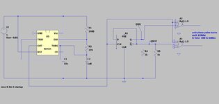
ICM7555 has a max frequency of 500kHz. (T=2us) However, pg 8 Fig 9 says there is a ~250ns propagation delay when vdd=5v.
That must mean that the duty cyle when at 500kHz must be limited to 0.75 maximum?
ICM7555
ICM7555 has a max frequency of 500kHz. (T=2us) However, pg 8 Fig 9 says there is a ~250ns propagation delay when vdd=5v.
That must mean that the duty cyle when at 500kHz must be limited to 0.75 maximum?
ICM7555