Welcome to our site! EDAboard.com is an international Electronics Discussion Forum focused on EDA software, circuits, schematics, books, theory, papers, asic, pld, 8051, DSP, Network, RF, Analog Design, PCB, Service Manuals... and a whole lot more! To participate you need to register. Registration is free. Click here to register now.
This is known as a current mirror. Whatever current level you have flowing in the left side of the circuit, that same level is duplicated in the right side as well.
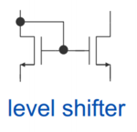
Perhaps it can be used in the role of level shifter, by a strategic arrangement of components.
Level shifting can be done by summing with a "fixed" constant current, which offsets the result by a "fixed" constant amount.
A current mirror is the ideal tool for that.
Hi,
For it to be a current mirror, the two transistors need to have the same Vgs. Here is the classification from the same article:
I have just attached the article.
If you go to slide 13 of that set, what he calls "level
shifter" is what I would call the cascode "guard" devices
(as opposed to the cascode "masters", your current
mirrors) in a cascode mirror stack. I doubt my
nomenclature is popular but have seen none I like better.
Here is what the paper says:
A common function of level shifter is to equilize the source potentials of its transistors. I think it is what it does in improved current mirror.
Slides 13 & 14 show the level shifter examples in a cascode current mirror, in the function of cascode "guard" devices, as dick_freebird called them above.
Slides 13 & 14 show the level shifter examples in a cascode current mirror, in the function of cascode "guard" devices, as dick_freebird called them above.
Sort of, in the sense that you move the usable range of
current-source (sink) common mode voltage up to
(Vs2+VT)Vs2+BVdss) at the drain of the "level shifter"
from (Vs1+VT)Vs1+BVdss) at the drain of the "current
mirror". Subject of course to other realities like Vgb, Vdb
limits in junction isolated technologies.
But often the use of this topology-nugget is not about
gaining a higher working voltage position, but controlling
the Vds swing of the current mirror to attain best match,
best PSRR, etc. Seldom is level shifting the primary goal,
in analog amplifier design, and you will see this form used
where no such gross level shifting is needed (although I
have also done some pretty tall stacks in low voltage SOI
that were all about the level shift, or more appropriately
the safe / reliable partitioning of working voltage).
It is interesting to know more about these basic building block.
There are some points from your post that I don't get. Could you explain more or give me some references?
ort of, in the sense that you move the usable range of
current-source (sink) common mode voltage up to
(Vs2+VT)Vs2+BVdss) at the drain of the "level shifter"
from (Vs1+VT)Vs1+BVdss) at the drain of the "current
mirror".
But often the use of this topology-nugget is not about
gaining a higher working voltage position, but controlling
the Vds swing of the current mirror to attain best match,
best PSRR, etc.
This site uses cookies to help personalise content, tailor your experience and to keep you logged in if you register.
By continuing to use this site, you are consenting to our use of cookies.

 Vs2+BVdss) at the drain of the "level shifter"