samuelyou
Newbie level 4
- Joined
- Jul 7, 2010
- Messages
- 6
- Helped
- 0
- Reputation
- 0
- Reaction score
- 0
- Trophy points
- 1,281
- Location
- china shanghai
- Activity points
- 1,333
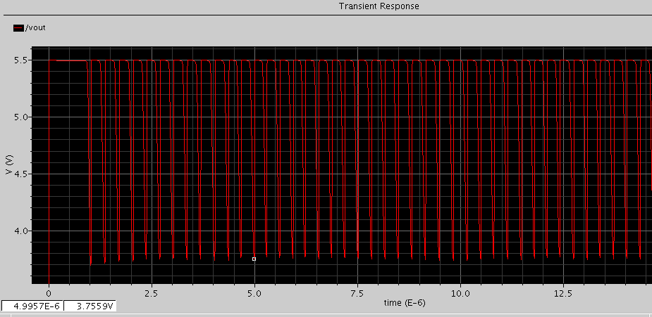
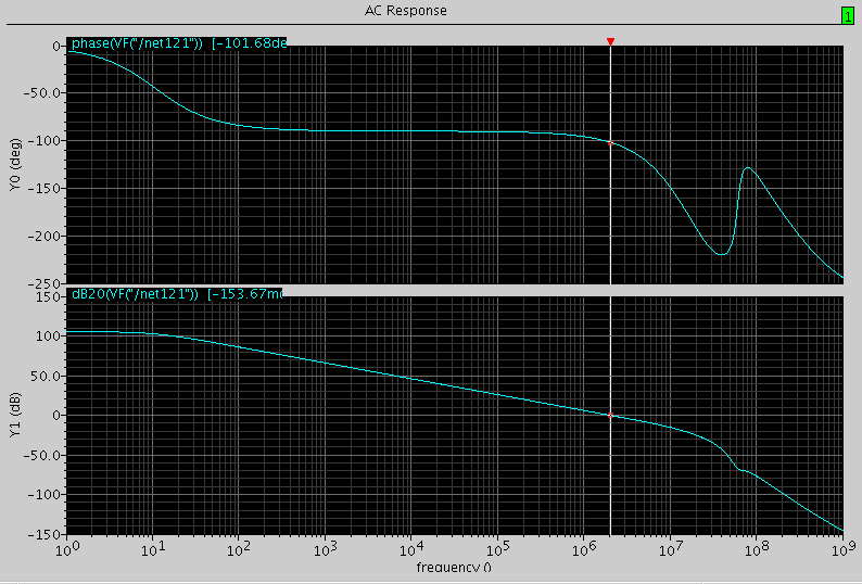
I would like to design a ldo with buffer, but some strange thing happened when I added the buffer. The phase margin is ok, but the transient simulation result show the output is oscillation. When I change the buffer to a VCVS, the transient oscillation disappear.
Please help to analysis why the transient oscillation. Thanks!
Added after 6 minutes:
Please help to analysis why the transient oscillation. Thanks!
Added after 6 minutes:
samuelyou said:I would like to design a ldo with buffer, but some strange thing happened when I added the buffer. The phase margin is ok, but the transient simulation result show the output is oscillation. When I change the buffer to a VCVS, the transient oscillation disappear.
Please help to analysis why the transient oscillation. Thanks!