Continue to Site

Welcome to EDAboard.com

Welcome to our site! EDAboard.com is an international Electronics Discussion Forum focused on EDA software, circuits, schematics, books, theory, papers, asic, pld, 8051, DSP, Network, RF, Analog Design, PCB, Service Manuals... and a whole lot more! To participate you need to register. Registration is free. Click here to register now.

LCRZ-Meter project(DDS signal source), large project with many questions/subjects.

Status
Not open for further replies.
Hi,

to get the information about the complex impedance of the load you need to simultaneously sample "voltage" and "current".

How many samples: Nyquist says at least twice the signal frequency. I recommend at least 4 samples per period. With 10MHz this means 40 Msamples/second. (are you able to do this?)

******
As i wrote before a lock in amplifier is far more simple. I used simple analog switches. then some Rs and Cs as low pass filters. The ADC can be very slow, because it simply has do measure about DC.

******
Anyway 10MHz is not that simple. Not with high speed ADC, nor with lock in amplifier. Expect a lot of error. In either case it needs a lot of experience to find the errors and cancel/calibrate them.

Klaus
 
  • Like
Reactions: Alloy

    Alloy

    Points: 2
    Helpful Answer Positive Rating
Hi Klaus.

I think I have missed or misread one of your posts, I will go back to read it again.

I am in the process of writing the guy whom designed the meter I have as some sort of reference to ask because I can't tell you how it's done but he has earlier stated that if he's technique is used(he hasn't claimed it as his own idea but I mean the one he used) then I can use a low speed ADC and all that would do is making the acquisition time longer.

As I think about it, 1MHz is my max frequency, so 2MSPS is the minimum needed and even if that isn't enough for the purpose of this meter 2MHz sample rate is still to fast for my taste, I think(and I may be wring) that it is preferable to allow the measurement algorithm to take much longer time to be performed if that in return gives a more manageable system and also perhaps decrease the errors.

Right now I have to run but when I return I will post a post showing the material I have found that is the "foundation" of my knowledge about what my system is going to have to include.
And I'll re read your post since I feel as I have obviously missed something.

Regards
 

How many samples: Nyquist says at least twice the signal frequency.

How that theorem is relevant here? That is useful when you need to transform a series from time domain to frequency domain (or vice-versa), correct? Here we are doing calculations on individual points
 

Hi,

I'd say you have to take care of nyquist in any case.

In the sentence before I mentioned "nyquist' i said:
to get the information about the complex impedance of the load you need to simultaneously sample "voltage" and "current".

I can't imagine how one can calculate the complex impedance of a 10MHz signal just with a single sample value of both voltage and current.
--> in my opinion it is essential to take a known number of voltage samples and their corresponding current samples to be able to calculate the voltage vector (length and angle) and the current vector (length and angle).
The sample rate usually should meet nyquist theorem.

For sure one can use "undersampling technique" ...with in a wide range varying input frequency it will be hard to calculate...

******
Individual points within an AC signal are about meaningless. Individual poins can be used for a DC signal (here when he uses the lock in amplifier).
I'd say even here nyquist (DC is 0 Hz) is true.

******
@David:
Nyquist says: MORE than twice the signal frequency.
So using 2.000.000 samples/second with a 1.000.000 Hz signal won't work.

And when you use 2.000.000 samples/second on a 999.000 Hz signal you need to take 2000 samples into account for full information.

You may use some Excel calculations/simulations to see what happens.

Klaus
 
  • Like
Reactions: David_

    David_

    Points: 2
    Helpful Answer Positive Rating
Before I go into the rest I just like to say that I have seriously begun to consider scraping the hole battery driven device idea.
I don't necessarily need to run it from a battery and considering the other challenges I ave before me I may be making it a little too hard for me by insisting on a battery driven device, better save that for another revision or project.


My inexperience with sampled data processing systems is one reason why I think that it is a good idea to make my power supply easier, I noticed that the solution with TPS65131 would not work out as I had thought. It's a IC containing one boost converter and one inverting converter that can if I use 5V as the power supply input to the IC manage +1A/-500mA out at +-6V, Both the switches(boost & inverting) has a current limit of 1950mA but that appears to result in output currents as I stated above where the positive rail can deliver twice what the negative rail can... I don't know why but it seems really clear when reading the datasheet and going through the design procedure.

Although I really don't like the idea of a bulky mains transformer, but considering that +-6V would be enough(centered tapped) followed by a positive and negative LDO each of which should be able to deliver 1A then the mains transformer may not be that large(a little more than 12VA). But I had hoped to solve it with some neat DC-DC converter. The ideal situation would be if I could fit the power supply inside the device which would call for a small space design and I am open for suggestions.

I was in a hurry when I wrote my last post but as far as I know the Nyquist fs/2 rule only applies for getting the frequency information of a square-wave, while if we where to look at a sinewave the same rule would still be true with the added result that if we want more than simply the frequency information of the sine-wave then fs/2 isn't really relevant and as Klaus keep referring to, 10MHz sample rate is what is needed to get the amplitude/phase information of a 1MHz sine-wave.

I have begun researching Lock-in Amplifiers and I have never known what they are, I thought it would be something like a smaller circuit element but now I know what it is and it sounds very interesting. Though it appears as a very big task to design such a circuit, that is not saying that I wouldn't want to go that way, I would find it as a very stimulation exercise but I am somewhat unclear about how a Lock-in Amplifier would be used to do what I want to do. As I read about the circuit I see how it relates to my objective but with very foggy eyes, I can't yet see through the over all confusion.

But if I where to ask my first question about Lock-in Amplifiers(LIAs) I would ask:
Does it appear suitable to you to use 2x AD9954(1 as the signal source to the DUT and then use the resulting waveform as the input signal and the other AD9954 as the reference input/phase shifter)?

A DDS like AD9954 does seem the ideal choice for a (LIA) due to its high frequency/phase resolution.

- - - Updated - - -

Nyquist says: MORE than twice the signal frequency.
So using 2.000.000 samples/second with a 1.000.000 Hz signal won't work.

And when you use 2.000.000 samples/second on a 999.000 Hz signal you need to take 2000 samples into account for full information.

You may use some Excel calculations/simulations to see what happens.
Klaus
By the way, maybe Matlab would be a good environment to look at those aspects?
I'm not sure why I ask because I think it is just that, I have gathered a collection of Matlab videos about signal processing that I will watch.
 
Last edited:

Hi,

as far as I know the Nyquist fs/2 rule only applies for getting the frequency information of a square-wave
This is wrong.
Square waves include overtones.
Sampling "square waves" sounds simple. But in detail it isn´t.
Nyquist is true for sine waves.
For example if you want to calaculate
* RMS value
* Phase shift
* or anything else,
then expect errors (gain error, offset error, fluctuating values...) when you don´t care about nyquist.

**************
and as Klaus keep referring to, 10MHz sample rate is what is needed to get the amplitude/phase information of a 1MHz sine-wave.
some additional information:
For a clean sinewave without overtones..
* two points per fullwave don´t give enough information.
* three points give full information.
But if you expect any distortion in your sine, then you should use a higher sample rate... like 10x your frequency.

****

Lock in amplifier:
You need a device (DDS, FPGA...) to generate your "test frequency". let´s say a 1MHz sine signal.
The (usual) lock in amplifier needs two square wave signals with exact 90° phase shift with respect to each other and it needs to be synchron to the test frequency.
Instead of two square waves I used 4 pieces of 90° (0°, 90°, 180°, 270°) shifted pulses (25% duty cycle) from my FPGA and simple CMOS switches.
The digital signals are essential.
If your DDS can produce the 2 or 4 digital signals (above) then you are on the safe side.
Some Rs and some Cs. and a slow ADC. That´s all. Not much effort and cheap.

The benefit it is that you don´t need high speed adcs anymore.
Math is (relatively) simple to get amplitude and phase shift.

Klaus
 
  • Like
Reactions: David_

    David_

    Points: 2
    Helpful Answer Positive Rating
Didn't review the preceding sample rate discussion from the start, but to mention a simple point: If the excitation signal is periodical with zero or low modulation bandwidth, undersampling is of course an option. Nyquist rate has to be related to the actual signal bandwidth, not the carrier frequency. https://en.wikipedia.org/wiki/Undersampling
 
  • Like
Reactions: David_

    David_

    Points: 2
    Helpful Answer Positive Rating
There is a sneaky way to do a network analyser (Which is basically what you are trying to design) that does NOT need high speed converters...

Basically, what you do is run two Oscillators with a known small frequency offset (maybe 1KHz) as follows:

Your first oscillator runs at the desired measurement frequency and feeds the device under test via a suitable pad, it also feeds one input of a mixer.

The second oscillator at say 1KHz above the desired measurement frequency feeds the other input of the mixer, and also feeds one input of a second mixer.

The output of the first mixer is lowpassed and the resulting 1KHz tone forms your reference channel.

The signal from the device under test is taken to the second mixer, where it is mixed with the second oscillator, again giving a 1KHz tone the amplitude and phase of which (Relative to the reference tone) can be used to derive the complex transmission parameters.

Obviously you can add more detector channels as required to do however many ports you feel are needed.

Thus your ADCs are now solidly audio band doings, and in fact if you sneakily make the ADCs run at exactly 4 times the difference frequency you can get an I/Q pair by simply taking alternate samples....

The easy way to produce the two RF sources with an exact frequency difference is of course a pair of DDS chips with a common clock, and you can improve performance if desired by using an RF rather then audio IF and filtering it heavily....

Regards, Dan.
 
  • Like
Reactions: David_

    David_

    Points: 2
    Helpful Answer Positive Rating
Hi,

Didn't review the preceding sample rate discussion from the start, but to mention a simple point: If the excitation signal is periodical with zero or low modulation bandwidth, undersampling is of course an option. Nyquist rate has to be related to the actual signal bandwidth, not the carrier frequency. https://en.wikipedia.org/wiki/Undersampling

I already mentioned undersampling.

With undersampling you may get good amplitude information.
But you may loose phase information.

(Indeed it is not "lost". It still is available, but i find it very difficult to calculate. You have to re-order the incoming sample values. And the "order" is not fixed, it is different for each test-frequency. Additionally for FFT or DFT you need a fixed number of samples. It does not depend on the DFT/FFT only. With undersampling it depends on the test-frequency also.)

****
@Dan
I know this undersampling technique.
Maybe a fixed frequency offset gives an improvement.
But gives it back the phase information 1:1?
And is it suitable for test frequencies from Hz to MHz?

To be true, I don´t know the exact answer(s), but i doubt both.

Klaus
 
  • Like
Reactions: David_

    David_

    Points: 2
    Helpful Answer Positive Rating
some additional information:
For a clean sinewave without overtones..
* two points per fullwave don´t give enough information.
* three points give full information.

A sine wave (a*sin(w*t+b)) is specified by amplitude and frequency. Two points are sufficient to determine the amplitude and the frequency.

The phase is sometimes important and we will need a reference to determine the phase. In such a case, three points are needed for the complete description.
 

Hi,

@c_mitra
I wonder:
A sine wave (a*sin(w*t+b)) is specified by amplitude and frequency. Two points are sufficient to determine the amplitude and the frequency.
How do you calculate amplitude and frequency?
Maybe with an example: Sample1 = 1V, sample2 = 2V
..I really don´t know how to calcualte it.
***

The phase is sometimes important and we will need a reference to determine the phase. In such a case, three points are needed for the complete description.
The OP wants to determine a complex load. LCRZ meter.

Frequency is known, because the OP generates it (with the use of a DDS..). Waveform is also known: sine.
So we need to know amplitude and phase shift.

--> Amplitude of U, amplitude of I. --> Z = amplitude(U)/amplitude(I)

Now we need phase shift:
--> usually U is the phase reference of I.

Then we can calculate R, and L or C

Klaus
 
  • Like
Reactions: David_

    David_

    Points: 2
    Helpful Answer Positive Rating
Hmm...

I feel as I am somewhat below these discussions, I will sketch the expressed ideas out and get back to you about it.

I seem to go through the same process each time I try to grasp a new concept in that I start of my research and soon I'll enter a state of confusion worse than that I normally exists in, that confusion then persists until I have read enough for enough days to start to get some grasp of what it is about. But as the state of mind is confusion it can take any number of days/weeks to get rid of it since I don't really know when I am on a path that leads forward or not.
And I wonder what has been expressed here now, or rather what does it mean for my application...

I think I have been presented with two different techniques to accomplish my goals while avoiding ADCs with sample rates of something like 10MHz/10MSPS, because that is the point of the Lock-in Amplifier idea in this situation right?

Because I was quite sure that going with the Opamp Auto-Balancing Bridge was a appropriate choice, and a choice that would be pretty simple in hardware(the software side is from my perspective a large problem to overcome in any of the scenarios), I don't mind changing my approach but I do have some problems in accessing the situation and I can definitively not deduce any Pro's vs Con's between the different suggestion(apart from the ADC sampling rate).

Could someone maybe elaborate your thoughts relating to which technique would be you choice and why?

I have started to read about Lock-in Amplifiers(LIO), both analog and digital LIOs and it appears apparent that there are no purely digital solution.
But I am not sure about what I need to do or where I should start, it seems as if there are so very many different kinds of LIO implementations, but I will try and draw a system illustration in order to define blocks that can be manage individually.

But what I was going for with this design was a design where the amplitude of the excitation signal could be varied in a linear fashion as well as having the option of introducing a DC-bias, the point of this isn't that I think that that will give me the best design but the best opportunity to understand and learn to more intuitively understand complex impedance and the amplitude/DC-bias adjustments are meant to revile to me what is important/influential and what is not, or something like that.

Would a LIO come get in my way regarding my desire for a adjustable excitation amplitude & DC-bias level?
The purpose of a Lock-in Amplifier are according to all sources to extract a small signal from an environment with a much larger noise/common-mode signal(related to the signal of interest) but that isn't why I would use a LIO, as far as I know this use of a LIO system could be conceptually be compared to the use of RF detectors, ei. solving the ADC speed issue by converting the AC sine-wave information to a DC signal to be interpreted.
 

Hi,

I think I have been presented with two different techniques to accomplish my goals while avoiding ADCs with sample rates of something like 10MHz/10MSPS, because that is the point of the Lock-in Amplifier idea in this situation right?
--> Yes, the benefit of the lock_in_amplifier is you don´t need 10Msamples ADC. The input to the ADC (= output of the filtered lock_in_amplifier) is almost DC, therefore 100 samples/second is enough. (no kilosamples, no megasamples). You may use a high resolution I2C or SPI ADC. But you get full amplitude and phase information.

going with the Opamp Auto-Balancing Bridge was a appropriate choice
Are you aware that with a (auto) balancing bridge ... you need to balance with a complex load.
Even with a bridge you have phase shift.... and the output of the bridge will never be zero (never be near zero) when you have a complex load and try to "balance" it with just a resistve load.

******
LIA:
I recommend the analog solution. Using cheap analog switches (CD4053, DG4053...) and simple Rs and Cs.
The main question is: You need to generate the test signal sine AND absolutely synchronously 2 digital signals 90° phase shifted to each other (or 4 signals 25% duty cycle 90° phase shifted)?
If this is not the case, then use another solution.
The precision of the LIA depends on the sine signal quality AND the digital signal quality.
I don´t say LIA is the one and only best solution.

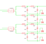
LIA_sch.pngLIA_BRD.png
Here you see my LIA solution with two 90° shifted digtial signals
And the BRD layout about 10mm x 24mm. 6 cheap devices. (because I used R-array and C array)

You need a LIA for voltage and a LIA for current for best results.
******

The LIA can handle a wide range of input voltage...thats what you wrote: even in a very noisy system it can precisely detect your excitation signal. Amplitude and phase.
And with the shown LIA schematic you even may be able to measure DC voltage (in an usual LIA this is not the case)

*****
But as already said: there are many ways to achieve your goal...

Klaus
 
  • Like
Reactions: David_

    David_

    Points: 2
    Helpful Answer Positive Rating
It would be one thing if using a LIA would decrease the speed by some degree, but given the speed I now know I can use if I go the LIA way a auto-balancing bridge does seem like a bad idea, a bad idea for someone at my level of knowledge at least and I don't have any particular journeying to tackle the difficulties of a 10MSPS system design...

Q1:
About the sine & digital signals, the AD9954 Complete DDS IC does contain a comparator with the intended purpose of turning the sine-wave into a square-wave which will precisely follow the Sine-waves frequency.
I could use the internal comparator to generate a square-wave and then use some sort of phase-shifting circuit to generate two versions of that square-wave with a 90° phase difference, do anyone know of a circuit to shift the phase of a square-wave by 90°?
Q1end

Q2:
About the DC-bias, it sounds as that may be no problem with a LIA design.
Unless I have misunderstood how this system is supposed to work it will work just fine since the only information needed about the DC-bias is how high a voltage/current I am applying to the DUT(and that would be supplied by ADC(s) within the DC-bias generator stage itself) and it would not matter if the LIA is a AC coupled circuit since the interesting part isn't what happens to the DC signal but rather how the DC-bias affects the complex impedance.
Though I feel fairly unsure about this, but from where I stand today this appears valid?
Q2end

Q3:
Then about the DDS signal source, I may be wrong but as I see it I should use as high a DDS system clock as possible(that would be 400MHz) in order to make the output filtering easy. If I use 400MHz DDS system clock then the first frequency component after the fundamental frequency would occur a little below 200MHz depending on my output frequency(let's assume that it occurs at 200MHz), then the filtering would not be particularly difficult and could be done by a Sallen-key Butterworth low-pass filter:
DDS_low-pass_filter.png
Do you agree?
Q3end

Q4:
I have some doubts about my signal chain regarding the DDS output, isn't there any way to get rid of the hole bunch of switchable resistors that are used to control the attenuation/gain of the signal by using a DAC & a opamp somehow?
Q4end

Q5:
When I through LTspice developed the filter above I couldn't get rid of the... gain is it? of the signal around 1MHz. The plot show around 400-500dBm higher than the lower part of the pass-band and that throws of my plans, at least it makes thing difficult.
I had planned to amplify the sine-wave to it's maximum amplitude, the system will be driven from ±5,5V using RRIO opamps and the sine-wave was to be amplified to above 5Vpeak and then go through a voltage divider in which the bottom resistor could be chosen to be 1 out of 16 values. I would amplify the sine to above 5Vpeak because the max amplitude I want is 5Vpeak and there will always be some attenuation with the voltage divider so then I make it so that the max setting attenuates the above 5Vpeak sine into a 5Vpeak sine precisely.
But the fact that at higher frequencies the signal amplitude will rise somewhat will mean that I won't get a accurate output amplitude, yes?

I often find my self very bothered with small things like that and I suspect that it is a aspberger related behavior, but in this case maybe it will not matter, will it?
Q5end

Q6:
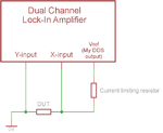
As far as I can deduce this is how a LIA instrument would be connected to perform Z measurements:
LIA-DUT_connection.png

And I am not able to see the following clearly, in fact I am totally lost. But is there a point in having a adjustable amplitude of the sine-wave as well as a selection of current limiting resistors to choose from?
Q6end
 

Hi,

To Q1:
The digital square wave signals influence precision. If there is no exact phase shift, or it is unstable somehow, then the results becoming less reliable. So this is critical.
A comparator solution and an analog exact 90° phase shift...especially with variable frequency....will become difficult.
On the other side the design with an high speed ADC wil be difficult, too.

To Q3:
An LT1007 is definitely too slow.
With that high frequencies I'd rely on passive filters.

To Q4:
You need to measure the stimulation signal, therefore it dies not need tobe very precise in amplitude.
Imagine if U is 20% too high, then I will also be 20% too high. But when dividing U/I ...the result is correct.

To Q6:
With or without the LIA you need to measure U and I somehow. But in your picture the Y input is grounded. It will see 0V.
For the known resistors use very low impedance ones. No wirewound!
(Out of curiosity I tested (as DUT) a wiewound resistor --> funny HF behaviour)

Klaus
 
  • Like
Reactions: David_

    David_

    Points: 2
    Helpful Answer Positive Rating
I have written a response to the last post posted, but I don't like how long my posts are and I want to ask 1 question before I ´go on with the response.

According to my previous plans(pre-LIA) I knew that there where going to be a critical timing issue to take care of regarding the DDS clock frequency and the ADC sampling rate or rather the ADC sampling timing.
With a LIA that obviously vanishes but I have been trying to get a prototype PCB done so that I can start developing the AD9954 driver and test out the DDS and start getting to grips with that.

And I want to be sure that I don't etch a PCB and solder on the pricey AD9954 only to discover that I missed some important detail about the clocks, before I had to figure out the frequency for a single crystal to be used both with the DDS(and it's internal PLL to get 400MSPS) and the XMEGA MCU/ADC. I'm not sure but it looks like with a LIA the the MCU can run at its own speed and the DDS clock doesn't matter apart from not being a integer multiple of a desired output frequency, so I will want to avoid a integer divisible clock frequency so that my 1MHz output will not be smothered with a lot of spurs and whatnot.

And I am really itching to get a PCB with the XMEGA/AD9954+part of it's output stage done since there will be quite a lot of work for me to get everything right in software.

Regards
 

So I have been playing around with a AD design tool that allows you to choose a DDS IC, a DDS clock frequency and optional filter and some other stuff and then look at the output in the frequency domain.

And I have been thinking about how to get rid of the harmonics but my conclusion is that I will never get rid of them, but then I thought "why would I care?", the beauty of the LIA is that the harmonics will not influence the LIA right?

I have never worked on anything that made harmonics relevant, not to me anyway but I am very unsure about this.

I don't understand what components of the DDS output that I would want to filter out and what pats I don't need to pay attention to?

Regards
 

Hi,

, but then I thought "why would I care?", the beauty of the LIA is that the harmonics will not influence the LIA right?
The output of the LIA is independent of even harmonics...
Unfortunately the output of the LIA will be influenced by the odd harmonics....and distortions are mainly odd harmonics....

The influence decreases with increasing harmonics frequency.

But usually the DDS shoukd be be relatively clean with low frequency harmonics....what does the datasheet say?

Klaus
 

I have been writing a post addressing the datasheet which i have problems understanding and have been writing since last night when Klaus answered, but the process of writing that post has lead me to some further research so I don't know when I'll answer but as soon as I can anyway.
 

While trying to get to writing about the last subject here I got my self into the power supply design and it really bothers me that I haven't completed it.
So let's switch focus towards that.

I have found a 2*6VAC secondary mains transformer which I hope is suitable to derive ±5,5V, I don't remember the VA number but it was specified to deliver something like 1250mA.

My power supply needs ±5,5V, +3,3V and 2 +1,8V rails, the +3,3V and one of the 1,8V rails are for the µC and the digital DDS supply and the ±5,5V and the other 1,8V supply is for analog parts so I have thought to separate those into a analog and a digital supply sections.

But I had thought to use a capacitance multiplier circuit to minimize the bulk capacitor size and minimize the ripple before the linear regulators but I can't get my LTspice capacitance multiplier to work properly, the following is just an illustration of the concept for my power supply:
LCRZ_Power_Supply2.png

The first problem is how to get a suitable voltage amplitude out of the capacitance multipliers, but then also I have a problem with the negative supply.

For the positive supply I will use a TL1963A which has a output voltage noise of 40µVrms(not taking the gain to get to 5,5V into consideration) but there are no negative equivalent that gives anyway near that low noise ´, yes there are but they are expensive IC's which I would prefer not to use.
The negative regulators I have looked at have output noises of sever hundred µVrms as opposed to 40µVrms of the positive regulator.

Does anyone have any suggestions or insights to this situation?

Regards

- - - Updated - - -

The problem with the LTspice circuit is that I can't figure out hoe the output voltage is managed, it is not a fixed relationship set by the zener + bjt voltage drop and the resistors are drastically impacting the output voltage in a way I haven't been able to grasp.
 

Status
Not open for further replies.

Part and Inventory Search

Welcome to EDABoard.com

Sponsor

Back
Top